EMERSONMVME6100 Single Board Computer Installation and Use
Overview of Contents
This manual is divided into the following chapters and appendices:
Chapter 1, Hardware Preparation and Installation, provides MVME6100 board preparation and
installation instructions, as well as ESD precautionary notes.
Chapter 2, Startup and Operation, provides the power-up procedure and identifies the switches
and indicators on the MVMEM6100.
Chapter 3, MOTLoad Firmware, describes the basic features of the MOTLoad firmware product.
Chapter 4, Functional Description, describes the MVME6100 on a block diagram level.
Chapter 5, Pin Assignments, provides pin assignments for various headers and connectors on
the MMVE6100 single-board computer.
Appendix A, Specifications, provides power requirements and environmental specifications.
Appendix B, Thermal Validation, provides information to conduct thermal evaluations and
identifies thermally significant components along with their maximum allowable operating
temperatures.
Appendix C, Related Documentation, provides a listing of related Emerson manuals, vendor
documentation, and industry specifications.
The MVME61006E Series Single-Board Computer Installation and Use manual provides the
information you will need to install and configure your MVME61006E single-board computer
(hereinafter referred to as MVME6100). It provides specific preparation and installation
information, and data applicable to the board.
As of the printing date of this manual, the MVME61006E supports the models listed below.
Abbreviations
Conventions
The following table describes the conventions used throughout this manual.
Model Number Description
MVME61006E-0161 1.267 GHz MPC7457 processor, 512MB DDR memory, 128MB Flash,
Scanbe handles
MVME61006E-0163 1.267 GHz MPC7457 processor, 512MB DDR memory,128MB Flash, IEEE
handles
MVME61006E-0171 1.267 GHz MPC7457 processor, 1GB DDR memory, 128MB Flash, Scanbe
handles
MVME61006E-0173 1.267 GHz MPC7457 processor, 1GB DDR memory, 128MB Flash, IEEE
handles
Notation Description
0x00000000 Typical notation for hexadecimal numbers (digits are
0 through F), for example used for addresses and
offsets
0b0000 Same for binary numbers (digits are 0 and 1)
bold Used to emphasize a word
Screen Used for on-screen output and code related elements
or commands in body text
Courier + Bold Used to characterize user input and to separate it
from system output
Reference Used for references and for table and figure
descriptions
File > Exit Notation for selecting a submenu
<text> Notation for variables and keys
Summary of Changes
This is the third edition of the Installation and Use manual. It supersedes the November 2007
edition and incorporates the following changes.
Comments and Suggestions
We welcome and appreciate your comments on our documentation. We want to know what
you think about our manuals and how we can make them better.
Mail comments to us by filling out the following online form:
http://www.emersonnetworkpowerembeddedcomputing.com/ > Contact Us > Online Form
In "Area of Interest" select "Technical Documentation". Be sure to include the title, part number,
and revision of the manual and tell us how you used it.
Part Number Date Changes
6806800D58E March 2009 Added csUserAltBoot command to Table "MOTLoad
Commands" on page 33 , editorial changes
6806800D58D April 2008 Updated to Emerson publications style.
6806800D58C January 2008 Updated to remove two incorrect sources of reset. See Reset
Control Logic on page 71. Table 5-13 on page 90 was updated
to indicate both possible uses of pins C1, C2, C3, C4, Z25, Z27,
Z29, and Z31 (when J30 is configured for rear Ethernet and
when J30 is configued for full PMC mode).
6806800D58B November
2007
Updated to better describe how to configure the VIO keying
pins for the PMC sites. See PMC I/O Voltage Configuration on
page 22. Also, Table 5-12 on page 89 was updated to identify
the Geographical Addressing pins on Row D of the P1
connector and minor updates were made to correct the hot
link to the literature catalog web site and update the reader
comments link.
Overview
This chapter contains the following information:
z Board preparation and installation instructions
z ESD precautionary notes
1.2 Description
The MVME6100 is a single-slot, single-board computer based on the MPC7457 processor, the
MV64360 system controller, the Tsi148 VME Bridge ASIC, up to 1 GB of ECC-protected DDR
DRAM, up to 128MB of flash memory, and a dual Gigabit Ethernet interface.
Front panel connectors on the MVME6100 board include: two RJ-45 connectors for the Gigabit
Ethernet, one RJ-45 connector for the asynchronous serial port with integrated LEDs for
BRDFAIL and CPU run indication, and a combined reset and abort switch.
The MVME6100 is shipped with one additional asynchronous serial port routed to an on-board
header.
The MVME6100 contains two IEEE1386.1 PCI, PCI-X capable mezzanine card slots. The PMC
slots are 64-bit capable and support both front and rear I/O. All I/O pins of PMC slot 1 and 46
I/O pins of PMC slot 2 are routed to the 5-row DIN, P2 connector. I/O pins 1 through 64 from
J14 of PMC slot 1 are routed to row C and row A of P2. I/O pins 1 through 46 from J24 of PMC
slot 2 are routed to row D and row Z of P2.
The MVME6100 has two planar PCI buses (PCI0 and PCI1). In order to support a more generic
PCI bus hierarchy nomenclature, the MV64360 PCI buses will be referred to in this document
as PCI bus 0 (root bridge instance 0, bus 0) and PCI bus 1 (root bridge instance 1, bus 0). PCI bus
1 connects to PMC slots 1 and 2 of the board. PCI bus 0 connects to the Tsi148 VME Bridge ASIC
and PMCspan bridge (PCI6520). This interface operates at PCI-X (133 MHz) speed. Both PCI
planar buses are controlled by the MV64360 system controller.
Voltage Input/Output (VIO) for PCI bus 1 is set by the location of the PMC keying pins; both pins
should be set to designate the same VIO, either +3.3V or +5V.
The MVME6100 board interfaces to the VMEbus via the P1 and P2 connectors, which use 5-row
160-pin connectors as specified in the VME64 Extension Standard. It also draws +12V and +5V
power from the VMEbus backplane through these two connectors. The +3.3V, +2.5V, +1.8V,
and processor core supplies are regulated on-board from the +5V power.
For maximum VMEbus performance, the MVME6100 should be mounted in a VME64x
compatible backplane (5-row). 2eSST transfers are not supported when a 3-row backplane is
used.
The MVME6100 supports multiple modes of I/O operation. By default, the board is configured
for Ethernet port 2 to the front panel (non-specific transition module), and PMC slot 1 in IPMC
mode. The board can be configured to route Ethernet port 2 to P2 and support MVME712M or
MVME761 transition modules. The front/rear Ethernet and transition module options are
configured by jumper block J30.
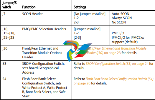
Selection of PMC slot 1 in PMC or IPMC mode is done by the jumper blocks J10, J15-J18, and
J25-J28 (see Table 1-2 on page 19). IPMC mode is selected when an IPMC712 or IPMC761
module is used. If an IPMC is used, J30 should be configured for the appropriate transition
module (see J30 configuration options as illustrated in Front/Rear Ethernet and Transition Module
Options Header (J30) on page 23).
The IPMC712 and IPMC761 use AD11 as the IDSEL line for the Winbond PCI-ISA bridge device.
This device supplies the four serial and one parallel port of the IPMC7xx module. The Discovery
II PHB (MV64360) does not recognize address lines below AD16. For this reason, although an
IPMC7xx module may be used on an MVME6100, the serial and parallel ports are not available,
nor addressable. This issue will be resolved at a later date.
Other functions, such as Ethernet and SCSI interfaces, are function independent of the
Winbond IDSEL line. The wide SCSI interface can only be supported through IPMC connector
J3.
PMC mode is backwards compatible with the MVME5100 and MVME5500 and is accomplished
by configuring the on-board jumpers.
1.3 Getting Started
This section provides an overview of the steps necessary to install and power up the
MVME6100 and a brief section on unpacking and ESD precautions.
Overview of Startup Procedures
The following table lists the things you will need to do before you can use this board and tells
where to find the information you need to perform each step. Be sure to read this entire
chapter, including all Caution and Warning notes, before you begin.
1.3.2 Unpacking Guidelines
Unpack the equipment from the shipping carton. Refer to the packing list and verify that all
items are present. Save the packing material for storing and reshipping of equipment.
Table 1-1 Startup Overview
What you need to do... Refer to...
Unpack the hardware. Unpacking Guidelines on page 17
Configure the hardware by setting jumpers on the board. Configuring the Hardware on page 18
Install the MVME6100 board in a chassis. Installing the Blade on page 27
Connect any other equipment you will be using Connecting to Peripherals on page 27
Verify the hardware is installed. Completing the Installation on page 28
If the shipping carton is damaged upon receipt, request that the carrier’s agent be present
during the unpacking and inspection of the equipment.
1.4 Configuring the Hardware
This section discusses certain hardware and software tasks that may need to be performed
prior to installing the board in a chassis.
To produce the desired configuration and ensure proper operation of the MVME6100, you may
need to carry out certain hardware modifications before installing the module.
Most options on the MVME6100 are software configurable. Configuration changes are made
by setting bits in control registers after the board is installed in a system.
Avoid touching areas of integrated circuitry; static discharge can damage circuits.
Emerson strongly recommends that you use an antistatic wrist strap and a conductive foam
pad when installing or upgrading a system. Electronic components, such as disk drives,
computer boards, and memory modules can be extremely sensitive to electrostatic
discharge (ESD). After removing the component from its protective wrapper or from the
system, place the component flat on a grounded, static-free surface (and, in the case of a
board, component side up). Do not slide the component over any surface.
If an ESD station is not available, you can avoid damage resulting from ESD by wearing an
antistatic wrist strap (available at electronics stores) that is attached to an active electrical
ground. Note that a system chassis may not be grounded if it is unplugged.
Inserting or removing modules with power applied may result in damage to module
components.
Dangerous voltages, capable of causing death, are present in this equipment. Use extreme
caution when handling, testing, and adjusting
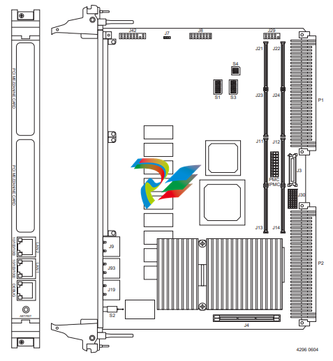
Jumpers/switches are used to control those options that are not software configurable. These jumper settings are described further on in this section. If you are resetting the board jumpers from their default settings, it is important to verify that all settings are reset properly. Figure 1-1 illustrates the placement of the jumpers, headers, connectors, switches, and various other components on the MVME6100. There are several manually configurable headers on the MVME6100 and their settings are shown in Table 1-2. Each header’s default setting is enclosed in brackets. For pin assignments on the MVME6100, refer to Chapter 5, Pin Assignments. Items in brackets are factory default settings.

The MVME6100 is factory tested and shipped with the configuration described in the following
sections

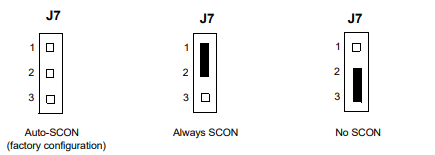
SCON Header (J7)
A 3-pin planar header allows the choice for auto/enable/disable SCON VME configuration. A
jumper installed across pins 1 and 2 configures for SCON always enabled. A jumper installed
across pins 2 and 3 configures for SCON disabled. No jumper installed configures for auto
SCON

PMC/IPMC Selection Headers (J10, J15 — J18, J25 — J28)
Nine 3-pin planar headers are for PMC/IPMC mode I/O selection for PMC slot 1. These nine
headers can also be combined into one single header block where a block shunt can be used as
a jumper.


