GEMVME51005E Single Board Computer Installation and Use
conductive foam pad when installing or upgrading a system.
Electronic components, such as disk drives, computer boards and memory
modules, can be extremely sensitive to electrostatic discharge (ESD). After
removing the component from its protective wrapper or from the system, place
the component on a grounded, static-free, and adequately protected working
surface. Do not slide the component over any surface. In the case of a Printed
Circuit Board (PCB), place the board with the component side facing up.
If an ESD station is not available, you can avoid damage resulting from ESD by
wearing an antistatic wrist strap (available locally) that is attached to an active
electrical ground.
Note A system chassis may not be a suitable grounding source if it is unplugged.
Preparation
This section includes subsections on hardware configuration that may need to be performed
immediately before and after board installation. It includes a brief reminder on setting bits in
control registers, setting jumpers for the appropriate configuration, and other VME data
considerations.
Hardware Configuration
To produce the desired board configuration and to ensure proper operation of the MVME5100, it
may be necessary to perform certain modifications before and after installation. The following
paragraphs discuss the preparation of the MVME5100 hardware components prior to installing
them into a chassis and connecting them.
A software readable header/ switch register (S1) is available on the MVME5100. This switch is not
defined by the hardware and it is shipped in the OFF position, as are all the switches on this board.
This S1 switch is available for user-specific configuration needs via the control registers.
The MVME5100 provides software control over most of its options by setting bits in control
registers. After installing it in a system, you can modify its configuration. For additional
information on the board’s control registers, refer to the MVME5100 Single Board Computer
Programmer's Reference Guide listed in Appendix D, Related Documentation.
It is important to note that some options are not software-programmable. These specific options
are controlled through manual installation or removal of jumpers, and in some cases, the addition
of other interface modules on the MVME5100. The following table lists the manually configured
jumpers on the MVME5100, and their default settings.
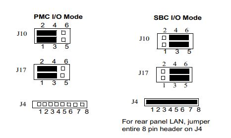
If you are resetting the board jumpers from their default settings, it is important to verify that all
settings are reset properly. For example, the SBC mode requires setting jumpers 4, 10 and 17 for
rear Ethernet functions, but it also requires resetting jumpers J6 and J20. Neglecting to reset J6 and
J20 could damage or destroy subsequent PMCs or PrPMCs installed on the base board at power-up.
Table 1-1. Manually Configured Headers/Jumpers
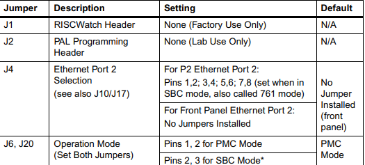
PMC/SBC (761/IPMC) Mode Selection
There are five headers associated with the selection of the PMC or SBC mode: J4, J6 J10,J17 and J20.
Three of these headers are responsible for secondary Ethernet I/O (J4, J10 and J17) to either the
front panel (PMC mode), or to the P2 connector via J4 (SBC mode). The other two headers (J6 and
J20) ensure proper routing of +/- 12V signal routing. The MVME5100 is set at the factory for front
panel I/O: PMC mode (see Table 1-1). The SBC mode should only be selected when using one of the
IPMC-7xx modules in conjunction with the corresponding MVME7xx transition module.
Installation Considerations
The MVME5100 draws power from the VMEbus backplane connectors P1 and P2. Connector P2 is
also used for the upper 16 bits of data in 32-bit transfers, and for the upper 8 address lines in
extended addressing mode. The MVME5100 will not function properly without its main board
connected to VMEbus backplane connectors P1 and P2.
Whether the MVME5100 operates as a VMEbus master or as a VMEbus slave, it is configured for 32
bits of address and 32 bits of data (A32/D32). However, it handles A16 or A24 devices in the
appropriate address ranges. D8 and/or D16 devices in the system must be handled by the
processor software.
If the MVME5100 tries to access off-board resources in a nonexistent location and if the system
does not have a global bus time-out, the MVME5100 waits indefinately for the VMEbus cycle to
complete. This will cause the system to lock up. There is only one situation in which the system
might lack this global bus time-out; that is when the MVME5100 is not the system controller and
there is no global bus time-out elsewhere in the system.
Note Software can also disable the bus timer by setting the appropriate bits in the Universe II
VMEbus interface.
Multiple MVME5100 boards may be installed in a single VME chassis; however, each must have a
unique VMEbus address. Other MPUs on the VMEbus can interrupt, disable, communicate with,
and determine the operational status of the processor(s).
Installation
This section discusses the installation of PMCs onto the MVME5100, installation of PMCspan
-
 HIRSCHMANN MSM20-M2M2M2M2SY9HH9E Ethernet media modul
 -
 HIRSCHMANN SPIDER-PL-20-05T1999999TWVHHHH Industrial Ethernet Rail Switch
 -
 Hirschmann SPIDER-PL-20-07T1M2M299TWVHHHH Industrial ETHERNET Rail Switch
 -
.png) Hirschmann (Belden) RS20-1600M2M2SDAEHC09.1.00 DIN-rail managed industrial Fast Ethernet switch
Hirschmann (Belden) RS20-1600M2M2SDAEHC09.1.00 DIN-rail managed industrial Fast Ethernet switch -
 Hirschmann (Belden) RS30-1602O6O6TDAPHC09.1.00 DIN-rail managed industrial Ethernet switch
 -
 Hirschmann (Belden) RS30-2402O6T1SDAPHH09.0.13 DIN-rail industrial Ethernet switch
 -
Hirschmann (Belden) SPIDER-PL-20-04T1S29999TY9HHHH Ethernet DIN-rail switch
-
 HIRSCHMANN RS20-1600T1T1SDAUHX Switch
 -
 HIRSCHMANN BRS42-0012OOOO-SPCZ99HHSES industrial switch
 -
 Hirschmann RS20-0800S2S2TDHPHH09.0.14 Fast Ethernet DIN rail switch.
 -
 HIRSCHMANN MM20-Z6Z6M2M2SAHH Hybrid Fast Ethernet Media Module
 -
 HIRSCHMANN MM20-Z6Z6T1T1SAHH hot-swappable hybrid Fast Ethernet Media Module
 -
 HIRSCHMANN MM20-P9P9T1T1SAHH Hybrid Fast Ethernet Media Module
 -
 HIRSCHMANN MM20-M4T1T1T1SAHH Hybrid Fast Ethernet Media Module
 -
 HIRSCHMANN MM20-M4M4T1T1SAHH Hybrid Fast Ethernet Media Module
 -
 HIRSCHMANN MM20-M2M2M2M2SZHH Ethernet media module
 -
HIRSCHMANN MM20-M2M2M2M2SAHH Ethernet media module
-
 HIRSCHMANN MM20-T1T1T1T1EBH 4-port Fast Ethernet Copper Cable Media Module
 -
HIRSCHMANN MM20-T1T1T1T1SAHH 4-port Fast Ethernet Copper Cable Media Module
-
HIRSCHMANN MM20-T1T1T1T1SAHH 4-port Fast Ethernet Copper Cable Media Module
-
 HIRSCHMANN MM20-Z6Z6EBH Hot-swappable fast Ethernet media module
 -
 HIRSCHMANN MM20-Z6Z6SAHH Ethernet media module
 -
HIRSCHMANN MM20-Z6Z6Z6Z6EBH Industrial Media Module
-
 MSM40-T1T1T1TZ9HH9E99.9.99 HIRSCHMANN Switch
 -
 HIRSCHMANN MS20-0800SAAEHC / MS20-0800SAAEHC0 8-port modular Layer 2 management Ethernet switch
 -
 Hirschmann RSPM20-4T14T1SZ9HHS9 Switch RSPM20-4T14T1SZ9HHS9
 -
 HIRSCHMANN RS20-1600M2M2SDAEHH09.1. RS20/30/40 Managed Switch configurator
 -
HIRSCHMANN RS20-1600M2M2SDAEHX09.0.00 Ethernet switch
-
 HIRSCHMANN BELDEN SPIDER-PL-20-07T1M2M299TY9HHHH / SPIDERPL2007T1M2M299TY9HHHH
 -
HIRSCHMANN MM3-1FXS2/3TX1 Switching Board Module
-
 HIRSCHMANN RSPE30-24044O7T99-ECCP999HHSE2A08.1.00 Industrial-grade fanless management-type Ethernet switch
 -
 HIRSCHMANN RS30-1602OOZZSDAEHC09.1.00 DIN-rail-mounted managed Layer 2 Ethernet switch
 -
 HIRSCHMANN MACH104-20TX-F Managed 24-port Full Gigabit 19" Switch
 -
 HIRSCHMANN Switch RS20-0800M4M4SDAE
 -
Hirschmann RS30-1602O6O6SDAEHH09.1. Management-type Ethernet switch
-
 Hirschmann RS30-1602OOZZSDAEHC09.0.10 Open rack-style Ethernet switch
 -
 HIRSCHMANN RSPE30-24044O7T99-SCCV999HHSI2SXX.X.XX High-Availability Seamless Redundancy
 -
HIRSCHMANN RSPE30-24044O7T99-SCCZ999HHSE2A DIN-rail Ethernet switch
-
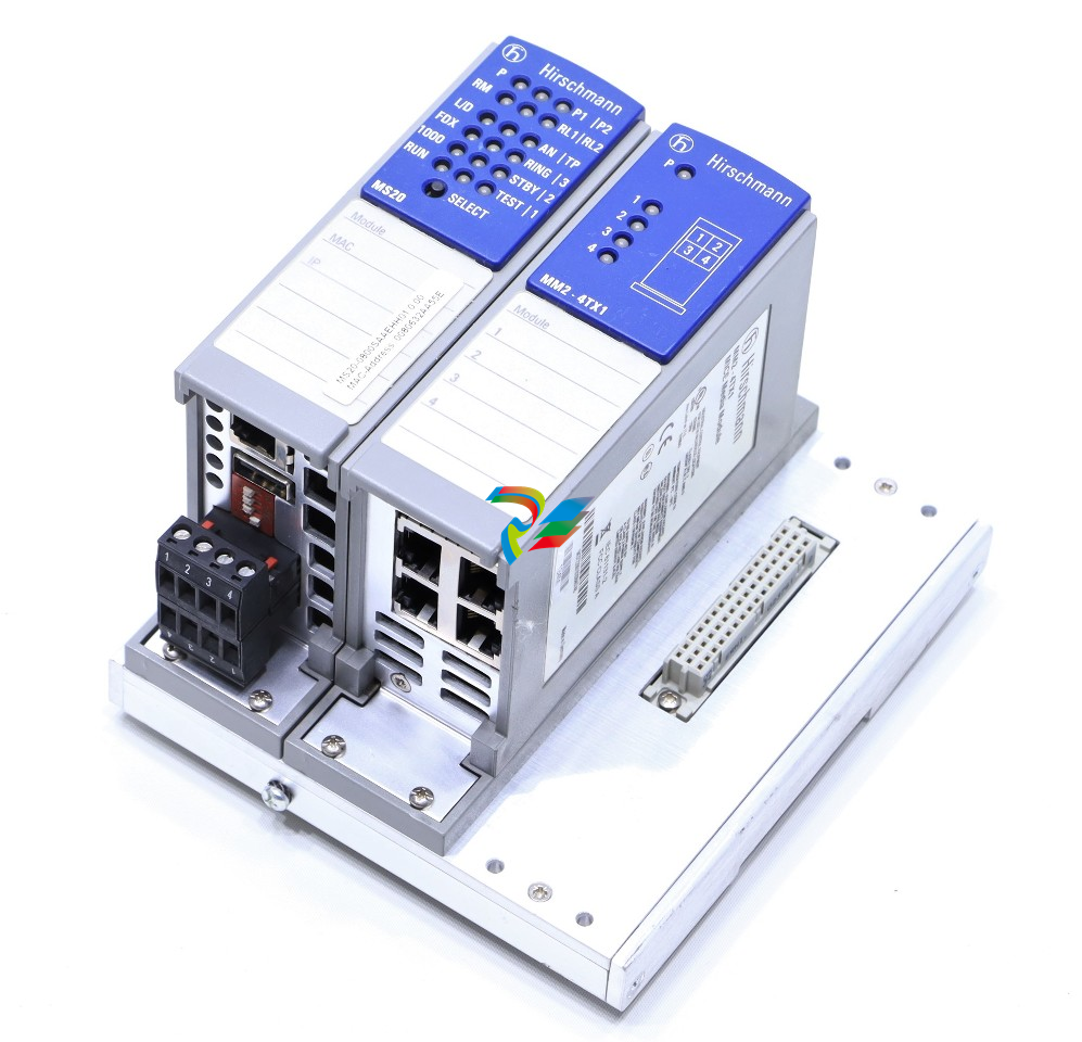
HIRSCHMANN MM2-4TX1-EEC switch
-
HIRSCHMANN MSM40-T1T1T1T1TZ9HH9E99.9.99 Module
-
 HIRSCHMANN RS20 Rail Switch RS20-0400S4T1SDAEHC07.1.01
 -
 HIRSCHMANN M4-FAST8-SFP Fast Ethernet media module
 -
 HIRSCHMANN RS20-0400M2T1SDAP Managed Fast-Ethernet-Switch
 -
 HIRSCHMANN BELDEN SPIDER II 8TX/1FX EEC Industrial Ethernet Rail Switch
 -
HIRSCHMANN MM3-2FXS2/2TX1
-
 HIRSCHMANN RS2-4TX/1FX EEC Industrial Ethernet Rail Switch
 -
 RS30-0802O6O6SDAEHC09.0.10 HIRSCHMANN Switch
 -
 HIRSCHMANN m4-8TP-RJ45 Ethernet Media Module
 -
 HIRSCHMANN MSP30-24040SCZ9URHHE3A switch
 -
 Hirschmann rack MS30-1602SAAPHC
 -
 HIRSCHMANN RS2-FX/FX Industrial Switch Module
 -
Rs1txfx - Hirschmann - Rs1-Tx/Fx Rail Switch
-
RS20-0800S2S2SDAEHC09.1.00 HIRSCHMANN Commutator
-
 Hirschmann EAGLE20 TX/TX Industrial Security Router
 -
 Hirschmann SPIDER-SL-20-04T1S29999SY9HHHH Industrial Switch
 -
 HIRSCHMANN MAR1040-4C4C4C4C9999SMMHRHHXX.X. Gigabit Ethernet Switch configurator
 -
 Hirschmann MAR1040 Industrial Switch
 -
 HIRSCHMANN BELDEN RS30-1602O6O6SDAE
 -
Hirschmann RS20-1600M2M2SDAUHC Ethernet DIN rail switch
-
 HIRSCHMANN OCTOPUS 24M industrial switch
 -
 HIRSCHMANN RS20-1600T1T1SDAE Management-type Ethernet switch
 -
 HIRSCHMANN RS20-1600T1T1SDAUHH industrial switch
 -
HIRSCHMANN RS20-0800M2M2SDAPHC09.0.04 switch
-
 Hirschmann MR 8-03 24V DC Industrial Modular Bridge/Router
 -
 HIRSCHMANN RS20-0400M2T1SDAPHC08.0.01 Managed Switch
 -
 MACH1130 Hirschmann Industrial Switch
 -
 HIRSCHMANN 943824-002 SPIDER 5TX Industrial Ethernet Switch
 -
 HIRSCHMANN RS30-0802O6O6SDAEHC09.1.00 Managed Industrial Switch
 -
 HIRSCHMANN RS20-0400M2M2TDAEHC04.0.01 Industrial Switch
 -
 HIRSCHMANN BRS20-0600Z6Z6-STCZ99HHSES Industrial Switch
 -
 HIRSCHMANN MACH104-20TX-FR-L3P Industrial Ethernet Switch
 -
 HIRSCHMANN RS40-0009CCCCEDBPHH06.0.01 Industrial Switch
 -
 HIRSCHMANN RS2-3TX/2FX EEC Industrial Ethernet Switch
 -
 Hirschmann MACH 1020/1030 Fast/Gigabit Rack Mount Switches
 -
HIRSCHMANN RS20-0800M2M2SDAPHC09.0.14 Industrial Switch
-
 HIRSCHMANN RS20-1600T1T1SDAEHC09.0.04 Industrial Switch
 -
 HIRSCHMANN RSB20-0800T1T1EAABHH Industrial Switch
 -
 HIRSCHMANN MACH4002-48+4G-L3E Industrial Backbone Switch
 -
 HIRSCHMANN RS20-0400S2T1SDAE Industrial Managed Switch
 -
HIRSCHMANN RS20-0800S2T1SDAUHC Industrial Switch
-
 HIRSCHMANN RS20-2400S4S4SDAEHC09.0.14 industrial switch
 -
 HIRSCHMANN OS20-001200T5T5T5- TBBZ999HHNE3S 08.1.00 industrial switch
 -
HIRSCHMANN OS20-001200T5T5T5- TBBZ999HHNE3S 08.1.00 industrial switch
-
 HIRSCHMANN RS40-0009CCCCSDAEHH09.0.14 switch
 -
 Hirschmann RS20-1600T1T1SDAUHC Management-type Ethernet Switch
 -
 Hirschmann M1-8SFP Switche
 -
Hirschmann Industrial Ethernet Ruggedized Switch MACH1000 Family
-
 Basler Electric, Solid State Protective Relay, BE1-60
 -
BASLER ELECTRIC SR4A-2B15B3A Static Voltage Regulator
-
.png) BASLER ELECTRIC EXCITER DIODE MONITOR EDM-200
BASLER ELECTRIC EXCITER DIODE MONITOR EDM-200 -
.png) BASLER ELECTRIC DECS125-15-B2C5 DIGITAL EXCITATION CONTROL SYSTEM V 2.0.9
BASLER ELECTRIC DECS125-15-B2C5 DIGITAL EXCITATION CONTROL SYSTEM V 2.0.9 -
 BASLER ELECTRIC BE1-851 OVERCURRENT PROTECTION RELAY MECHANISM
 -
 Basler Electric BE1-51A / BE151A
 -
 Basler Electric BE1-40Q Loss of Excitation Relay
 -
 Basler Electric BE1-87G Variable Percentage Differential Relay
 -
 Basler Electric BE1-11 Protection System I5A3M2P2N0EA00
 -
 BASLER ELECTRIC DECS-200-1C Digital Excitation Control System
 -
 Basler Electric / Kohler BE1-11g Generator Protection Relay G5A3M2J2N0E000
 -
BASLER ELECTRIC DECS125-15 DIGITAL EXCITATION CONTROL SYSTEM
-
 BASLER ELECTRIC BE1-951 OverCurrent Protecton System
 -
Basler Electric DECS-200-1L Digital Excitation Control System
-
 Basler Electric DGC-2020HD-5NS1DNSBA Digital Genset Controller -
 -
 BASLER ELECTRIC BE1-81T1EE1WA0N1F / BE181T1EE1WA0N1F
 -
 BASLER ELECTRIC BE1-25M1EA6PN5R1F / BE125M1EA6PN5R1F
 -
 BASLER ELECTRIC DECS-250-LN1SN1N DIGITAL EXCITATION CONTROL SYSTEM
 -
Basler Electric DECS-250-CN2CN 1N Digital Excitation Control System Unit
-
 BASLER ELECTRIC DECS-300-C0N0 DIGITAL EXCITATION CONTROL SYSTEM
 -
 BASLER ELECTRIC BE1-87T-A1E-A1J-D0S1F / BE187TA1EA1JD0S1F
 -
BASLER ELECTRIC BE1-11-G6D1M0J2P0E000 Protection System
-
 BASLER ELECTRIC BE1-GPS100-E4N1H1N GENERATOR PROTECTION SYSTEM
 -
 Jaquet Relay card (Auxiliary module) FTV 3090 377Z-03985
 -
 Jaquet Trip Chain Control card FTBU 3034 377Z-05030
 -
 Jaquet with input card -E04 FTFU 3024 -E04 377Z-05855
 -
 Jaquet with input card -E03 FTFU 3024- E03 377Z-03983
 -
 Jaquet FTFU 3024- E02 377Z-03982 with input card -E02
 -
 Jaquet FTFU 3024-E01 377Z-03981 with input card -E01
 -
 Hirschmann RS20-2400T1T1SDAE Industrial Managed Ethernet Switch
 -
 Hirschmann BELDEN EAGLE30-04022O6TT999SCCV9HSE3F
 -
 Hirschmann MM3-2FXS2/2TX MICE Media Module
 -
 Hirschmann RS20-1600M2M2SDAPHC08.0.05 Industrial Managed Switch
 -
 Hirschmann OZD Profi 12M G12-1300 PRO Fieldbus Repeater
 -
Hirschmann SPIDER 4TX/1FX-ST EEC Industrial Ethernet Switch
-
 Hirschmann MM2-2FXM3/2TX1 MICE Media Module
 -
 Hirschmann RS20-2400M2M2SDAPHC09.0.14 Industrial Switch
 -
 Hirschmann RS20-0400M2M2SDAEHC07.1.05 OpenRail Switch
 -
 Hirschmann OZD Profi 12M G12-EEC Fieldbus Repeater
 -
HIRSCHMANN MDA422-1/2-3.5c-23/46 sensor
-
Hirschmann RS30-2402T1T1SDAUHC Managed Industrial Switch