
EMERSONMVME55006E Single-Board Computer Installation and Use
ESD
Emerson strongly recommends that you use an antistatic wrist strap and a
conductive foam pad when installing or upgrading a system. Electronic components,
such as disk drives, computer boards, and memory modules can be extremely
sensitive to electrostatic discharge (ESD). After removing the component from its
protective wrapper or from the system, place the component flat on a grounded,
static-free surface (and, in the case of a board, component side up). Do not slide the
component over any surface.
If an ESD station is not available, you can avoid damage resulting from ESD by
wearing an antistatic wrist strap (available at electronics stores) that is attached to an
active electrical ground. Note that a system chassis may not be grounded if it is
unplugged.
Personal Injury or Death
Dangerous voltages, capable of causing death, are present in this equipment.
Use extreme caution when handling, testing, and adjusting.
Configuring the Hardware
This section discusses certain hardware and software tasks that may need to be performed
prior to installing the board in a chassis.
To produce the desired configuration and ensure proper operation of the MVME5500, you may
need to carry out certain hardware modifications before installing the module.
Most options on the MVME5500 are software configurable. Configuration changes are made
by setting bits in control registers after the board is installed in a system.
Jumpers and switches are used to control those options that are not software configurable.
These settings are described further on in this section. If you are resetting the board jumpers
or switches from their default settings, it is important to verify that all settings are reset properly.
Configuring the Board
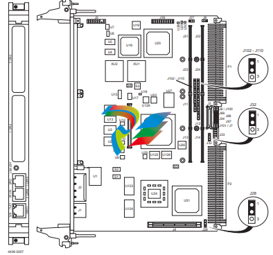
Figure 1-1 illustrates the placement of the jumpers, headers, switches, connectors, and various
other components on the MVME5500. There are several manually configurable headers and
switches on the MVME5500 and their settings are shown in Table 1-2. Each default setting is
enclosed in brackets. For pin assignments on the MVME5500, refer to Chapter 5, Connector
Pin Assignments.
Table 1-2 MVME5500 Jumper Settings

The MVME5500 is factory tested and shipped with the configuration described in the following
section.
1.6.2 Ethernet 2, PMC/SBC Mode, and P2 I/O Selection Headers (J6,
J7, J28, J32, J34, J97 – J110)
All of the headers described below are used in conjunction with each other to select various
modes of operation for 10/100BaseT Ethernet, PMC/SBC mode, and P2 I/O mode.
1.6.2.1 Ethernet
Four 3-pin planar headers (J6, J7, J100, J101) and four 2-pin planar headers (J34, J97, J98,
J99) are for 10/100/BaseT Ethernet 2 selection.
Ethernet 1 is the Gigabit Ethernet port and is front panel only.
Figure 1-1 MVME5500 Board Layout
For J6, J100, J7 and J101, install jumpers across pins 2-3 on all four headers for rear P2
Ethernet. For front-panel Ethernet, install jumpers across pins 1-2 on all four headers.
For J34, J97, J98 and J99, no jumpers are installed for front-panel Ethernet. For rear P2
Ethernet, install jumpers across pins 1-2 on all four headers when in SBC/IPMC761 mode.
1.6.2.2 PMC/SBC Mode Selection
The MVME5500 is set at the factory for PMC mode. The SBC/IPMC761 mode should only be
selected when using the IPMC761 module in conjunction with the MVME761 transition
module.The PMC mode should be selected when using PMC modules with specific user I/O in
conjunction with the corresponding transition module. PMC mode should also be selected when
using PrPMC modules.
Two 3-pin planar headers (J28, J32) control the supply of +/- 12 volts to the P2 connector; one
or both of these voltages are required by the MVME712 or MVME761 module when operating
in SBC mode. For PMC mode, jumpers are installed across pins 1-2 on both headers. For
SBC/IPMC761 mode, install jumpers across pins 2-3 on both headers. For SBC/IPMC712
mode, install a jumper across pins 2-3 for J32 and install a jumper across pins 1-2 for J28
Product Damage
When J28 is configured for SBC/IPMC mode, –12V is supplied to P2 pin A30. If there
is an incompatible board plugged into this P2 slot, damage may occur.
When J32 is configured for SBC/IPMC mode, +12V is supplied to P2 pin C7. If there is
an incompatible board plugged into this P2 slot, damage may occur.
P2 I/O Selection
Nine 3-pin planar headers (J102 –J110) are for P2 I/O selection. Jumpers are installed across
pins 1-2 on all nine headers when in PMC mode. Install jumpers across pins 2-3 on all nine
headers when in SBC/IPMC761 or SBC/IPMC712 mode to connect the extended SCSI signals
to P2
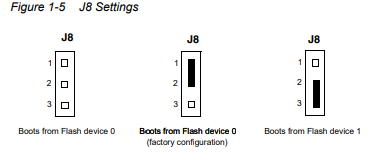
Flash Boot Bank Select Header (J8)
A 3-pin planar header selects the boot Flash bank. No jumper or a jumper installed across pins
1-2 selects Flash 0 as the boot bank. A jumper installed across pins 2-3 selects Flash 1 as the
boot bank.
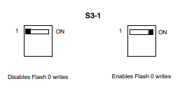
Flash 0 Programming Enable Switch (S3-1)
This switch enables/disables programming of Flash 0 as a means of protecting the contents
from being corrupted. The switch set to OFF disables all Flash 0 programming. The switch set
to ON enables the programming, this is the factory setting
Safe Start ENV Switch (S5-1)
This switch selects programmed or safe start ENV settings. When set to OFF, it indicates that
the programmed ENV settings should be used during boot. Set to ON indicates that the safe
ENV settings should be used.

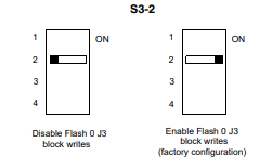
Flash 0 Block Write Protect Switch (S3-2)
This switch supports the Intel J3 Flash family write protect feature. Set to OFF, it enables the
lock-down mechanism. Blocks locked down cannot be unlocked with the unlock command. The
switch must be set to ON in order to override the lock-down function and enable blocks to be
erased or programmed through software. Refer to the Intel J3 Flash data sheet, listed in
Appendix C, Related Documentation, for further details.
SROM Initialization Enable Switch (S5-2)
This switch enables/disables the GT-64260B SROM initialization. When set to 2, it enables the
GT-64260B device initialization via I2C SROM. Set to ON disables this initialization sequence

PCI Bus 0.0 Speed Switch (S4-1)
This switch can force PCI bus 0.0 to run at 33 MHz rather than the standard method of allowing
the PMC board to control whether the bus runs at 33 MHz or 66 MHz. Set to 1, it allows the
PMC board to choose the PCI 0.0 bus speed. Set to ON forces PCI bus 0.0 to run at 33 MHz

VME SCON Select Header (J27)
A 3-pin planar header allows the choice for auto/enable/disable SCON VME configuration. A
jumper installed across pins 1-2 configures for SCON disabled. A jumper installed across pins
2-3 configures for auto SCON. No jumper installed configures for SCON always enabled.
PCI Bus 1.0 Speed Switch (S4-2)
This switch can force PCI bus 1.0 to run at 33 MHz rather than the standard method of allowing
the PMC board to control whether the bus runs at 33 MHz or 66 MHz. Set to 1, it allows the
PMC board to choose the PCI 1.0 bus speed. Set to ON forces PCI bus 1.0 to run at 33 MHz
EEPROM Write Protect Switch (S3-3)
This switch enables/disables programming of the on-board EEPROMs as a means of protecting
the contents from being corrupted. Set to 1, it disables EEPROM programming by driving the
WP pin to a logic high. Set to ON to program any of the EEPROMs at addresses A0, A6, A8,
and/or AA.
Setting the PMC Vio Keying Pin
Signalling voltage (Vio) is determined by the location of the PMC Vio keying pin. Each site can
be independently configured for either +5V or +3.3V signalling. The option selected can be
determined by observing the location of the Vio keying pin.
Figure 1-13 S3-3 Settings
Disables EEPROM Enables EEPROM programming
programming (factory configuration)

Installing the RAM5500 Module
Procedure
To upgrade or install a RAM5500 module, refer to and proceed as follows:
1. Attach an ESD strap to your wrist. Attach the other end of the ESD strap to the
chassis as a ground. The ESD strap must be secured to your wrist and to ground
throughout the procedure.
2. Perform an operating system shutdown. Turn the AC or DC power off and remove
the AC cord or DC power lines from the system. Remove the chassis or system
cover(s) as necessary for access to the VME boards.
3. Carefully remove the MVME5500 from its VME card slot and lay it flat, with
connectors P1 and P2 facing you.
4. Inspect the RAM5500 module that is being installed on the MVME5500 host board
to ensure that standoffs are installed in the four mounting holes on the module.
5. With standoffs installed in the four mounting holes on the RAM5500 module, align
the standoffs and the P1 connector on the module with the four holes and the P4
connector on the MVME5500 host board and press the two connectors together
until they are firmly seated in place.
7. Reinstall the MVME5500 assembly in its proper card slot following the procedure in
the next section. Be sure the host board is well seated in the backplane connectors.
Do not damage or bend connector pins.
8. Replace the chassis or system cover(s), reconnect the system to the AC or DC
power source and turn the equipment power on.
1.8 Installing PMCs
This section discusses the installation of a PMC module onto the MVME5500 and the
installation of a primary and secondary PMCspan module onto the PMC/MVME5500 processor
module.
If you have ordered one or more of the optional RAM500 memory mezzanine boards for the
MVME5500, ensure that they are installed on the board prior to proceeding. If they have not
been installed by the factory, and you are installing them yourself, please refer to Installing the
RAM5500 Module on page 28 for installation instructions. It is recommended that the memory
mezzanine modules be installed prior to installing other board accessories, such as PMCs,
IPMCs or transition modules.
1.8.1 Mounting the PMC Module
PMC modules mount on top of the MVME5500. Perform the following steps to install a
PMCmodule on your MVME5500.
Personal Injury or Death
Dangerous voltages, capable of causing death, are present in this equipment.
Use extreme caution when handling, testing and adjusting.
Product Damage
Inserting or removing modules with power applied may result in damage to module
components.
Avoid touching areas of integrated circuitry, static discharge can damage these
Procedure
This procedure assumes that you have read the user’s manual that came with your PMCs.
1. Attach an ESD strap to your wrist. Attach the other end of the ESD strap to an
electrical ground. Note that the system chassis may not be grounded if it is
unplugged. The ESD strap must be secured to your wrist and to ground throughout
the procedure.
2. Perform an operating system shutdown. Turn the AC or DC power off and remove
the AC cord or DC power lines from the system. Remove chassis or system cover(s)
as necessary for access to the VME modules.
3. If the MVME5500 has already been installed in a VMEbus card slot, carefully
remove it as shown in Figure 1-17 and place it with connectors P1 and P2 facing
you. Remove the filler plate(s) from the front panel of the MVME5500.
4. Insert the appropriate number of Phillips screws (typically 4) from the bottom of the
MVME5500 into the standoffs on the PMC module and tighten the screws (refer to
Figure 1-15).
5. Align the PMC module’s mating connectors to the MVME5500’s mating connectors
and press firmly into place.
1.8.2 Primary PMCspan
To install a PMCspan26E-002 PCI expansion module on your MVME5500, perform the
following steps while referring to the figure on the next page:
Figure 1-15 Typical Placement of a PMC Module on a VME Module

Procedure
This procedure assumes that you have read the user’s manual that was furnished with your
PMCspan.
1. Attach an ESD strap to your wrist. Attach the other end of the ESD strap to an
electrical ground. Note that the system chassis may not be grounded if it is
unplugged. The ESD strap must be secured to your wrist and to ground throughout
the procedure.
2. Perform an operating system shutdown. Turn the AC or DC power off and remove
the AC cord or DC power lines from the system. Remove chassis or system cover(s)
as necessary for access to the VME modules.
3. If the MVME5500 has already been installed in a VMEbus card slot, carefully
remove it as shown in Figure 1-17 and place it with connectors P1 and P2 facing
you.
4. Attach the four standoffs to the MVME5500. For each standoff:
Insert the threaded end into the standoff hole at each corner of the MVME5500 and
thread the locking nuts into the standoff tips and tighten.
5. Place the PMCspan on top of the MVME5500. Align the mounting holes in each
corner to the standoffs and align PMCspan connector P4 with MVME5100
connector J25.
Figure 1-16 PMCspan Installation on a VME Module

6. Gently press the PMCspan and MVME5500 together and verify that P4 is fully
seated in J4.
7. Insert four short screws (Phillips type) through the holes at the corners of the
PMCspan and into the standoffs on the MVME5500. Tighten screws securely.
1.8.3 Secondary PMCspan
The PMCspanx6E-010 PCI expansion module mounts on top of a PMCspanx6E-002. To install
a PMCspanx6E-010, perform the following steps while referring to the figure on the next page:
Personal Injury or Death
Dangerous voltages, capable of causing death, are present in this equipment.
Use extreme caution when handling, testing and adjusting.
Product Damage
Inserting or removing modules with power applied may result in damage to module
components.
Avoid touching areas of integrated circuitry, static discharge can damage these
circuits.
Procedure
This procedure assumes that you have read the user’s manual that was furnished with the
PMCspan, and that you have installed the selected PMC modules on your PMCspan according
to the instructions provided in the PMCspan and PMC manuals.
1. Attach an ESD strap to your wrist. Attach the other end of the ESD strap to an
electrical ground. Note that the system chassis may not be grounded if it is
unplugged. The ESD strap must be secured to your wrist and to ground throughout
the procedure.
2. Perform an operating system shutdown. Turn the AC or DC power off and remove
the AC cord or DC power lines from the system. Remove chassis or system cover(s)
as necessary for access to the VME module
3. If the Primary PMC Carrier Module and MVME5500 assembly is already installed in
the VME chassis, carefully remove it as shown in Figure 1-17 and place it with
connectors P1 and P2 facing you.
4. Remove four screws (Phillips type) from the standoffs in each corner of the primary
PCI expansion module.
5. Attach the four standoffs from the PMCspanx6E-010 mounting kit to the
PMCspanx6E-002 by screwing the threaded male portion of the standoffs in the
locations where the screws were removed in the previous step.
6. Place the PMCspanx6E-010 on top of the PMCspanx6E-002. Align the mounting
holes in each corner to the standoffs and align PMCspanx6E-010 connector P3 with
PMCspanx6E-002 connector J3.
7. Gently press the two PMCspan modules together and verify that P3 is fully seated
in J3.
8. Insert the four screws (Phillips type) through the holes at the corners of
PMCspanx6E-010 and into the standoffs on the primary PMCspanx6E-002. Tighten
screws securely.
The screws have two different head diameters. Use the screws with the smaller
heads on the standoffs next to VMEbus connectors P1 and P2.
You are now ready to install the module into the VME chassis. Follow the procedure, Installing
the Board on page 33.
Installing the Board
Procedure
Use the following steps to install the MVME5500 into your computer chassis.
1. Attach an ESD strap to your wrist. Attach the other end of the ESD strap to an
electrical ground (refer to Unpacking Guidelines). The ESD strap must be secured
to your wrist and to ground throughout the procedure.
2. Remove any filler panel that might fill that slot.
3. Install the top and bottom edge of the MVME5500 into the guides of the chassis.
Only use injector handles for board insertion to avoid damage/deformation to the
front panel and/or PCB.
4. Ensure that the levers of the two injector/ejectors are in the outward position.
5. Slide the MVME5500 into the chassis until resistance is felt.
6. Simultaneously move the injector/ejector levers in an inward direction.
7. Verify that the MVME5500 is properly seated and secure it to the chassis using the
two screws located adjacent to the injector/ejector levers.
8. Connect the appropriate cables to the MVME5500.
1.9.1 Connection to Peripherals
When the MVME5500 is installed in a chassis, you are ready to connect peripherals and apply
power to the board.
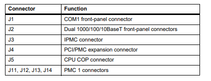
Figure 1-1 on page 20 shows the locations of the various connectors while Table 1-3 lists them
for you. Refer to Chapter 5, Connector Pin Assignments for the pin assignments of the
connectors listed below.
If a PMC module is plugged into PMC slot 1, the memory mezzanine card cannot be used
because the PMC module covers the memory mezzanine connector.
Figure 1-17 Installation into a Typical VME Chass

Completing the Installation
Verify that hardware is installed and the power/peripheral cables connected are appropriate for
your system configuration.
Replace the chassis or system cover, reconnect the system to the AC or DC power source, and
turn the equipment power on.
1.10 Startup and Operation
This section gives you information about:
z The power-up procedure
z Switches and indicators
1.11 Applying Power
After you verify that all necessary hardware preparation is complete and all connections are
made correctly, you can apply power to the system.
When you are ready to apply power to the MVME5500:
z Verify that the chassis power supply voltage setting matches the voltage present in the
country of use (if the power supply in your system is not auto-sensing)
z On powering up, the MVME5500 brings up the MotLoad prompt, MVME5500>
1.12 Switches and Indicators
The MVME5500 board provides a single push button switch that provides both Abort and Reset
(ABT/RST) functions. When the switch is depressed for less than three seconds, an abort
interrupt is generated to the processor. If the switch is held for more than three seconds, a
board hard reset is generated.
The MVME5500 has two front-panel indicators:
z BFL, software controlled. Asserted by firmware (or other software) to indicate a
configuration problem (or other failure).
z CPU, connected to a CPU bus control signal to indicate bus activity.
The following table describes these indicators:
Table 1-4 Front-Panel LED Status Indicators
Function Label Color Description
CPU Bus Activity CPU Green CPU bus is busy.
Board Fail BFL Yellow Board has a failure.
Functional Description
2.1 Overview
This chapter describes the MVME5500 on a block diagram level.
2.2 Block Diagram
Table 2-1 shows a block diagram of the overall board architecture.
Figure 2-1 Block Diagram

Features
The following table lists the features of the MVME5500.
Table 2-1 MVME5500 Features Summary

Processor
The MVME5500 supports the MPC7457 processor in the 483-pin CBGA package. The
processor consists of a processor core, an internal 256KB L2 and an internal L3 tag and
controller, which supports a backside L3 cache.
2.5 L3 Cache
The MVME5500 uses two 8Mb DDR synchronous SRAM devices for the processor’s L3 cache
data SRAM. This gives the processor a total of 2MB of L3 cache. These SRAM devices require
a 2.5V core voltage. The MVME5500 provides 1.5V as the SRAM I/O voltage. The L3 bus
operates at 200 MHz.
2.6 System Controller
The GT-64260B system controller for PowerPC architecture processors is a single chip solution
that provides the following features:
z A 64-bit interface to the CPU bus
z A 64-bit SDRAM interface
z A 32-bit generic device interface for Flash, etc.
z Two 64-bit, 66 MHz PCI bus interfaces
z Three 10/100Mb Ethernet MAC ports (two ports not used)
z A DMA engine for moving data between the buses
z An interrupt controller
z An I2C device controller
z PowerPC bus arbiter
z Counter/timers
-
 AMAT 0100-00046 AC Current Sense PWB
 -
 AMAT A0414720 Precision Advanced System Controller
 -
 AMAT 0010-00017 Precision Semiconductor Process Interface
 -
 AMAT 01-82889-00 High-Performance Semiconductor Component
 -
 ABB Sample Gas Cooler SCC-C 23070-0-10232110
 -
 IBA ibaRackline-PCHD Efficient process analysis with ibaHD-Server
 -
IBA ibaRackline-PC CAM Frame-accurate video information with ibaCapture
-
IBA ibaRackline-PC Highly available and reliable
-
 IBA Optical Signal Multiplier ibaBM-FOX-i-3o-D
 -
 IBA Optical Data Distribution System ibaBM-DIS-i-8o
 -
IBA Optical Data Concentrator ibaBM-COL-8i-o
-
 IBA ibaNet750-BM-D Acquisition via FO
 -
 IBA ibaW-750 Acquisition via Ethernet
 -
 IBA ibaPADU-8AI-I Compact Measurement Modules
 -
 IBA ibaPADU-D-8AI-I Compact Measurement Modules
 -
 IBA ibaPADU-8AI-U Compact Measurement Modules
 -
 IBA ibaPADU-D-8AI-U Compact Measurement Modules
 -
 IBA ibaPADU-4-AI-U Compact Measurement Modules
 -
 IBA ibaPADU-C-8AI Self-Supplied Data Logger
 -
 IBA ibaBM-ENetIP Bus monitor for EtherNet/IP
 -
 IBA ibaBM-eCAT Bus monitor for EtherCAT
 -
 IBA ibaBM-DP Bus monitor for PROFIBUS
 -
 IBA ibaBM-PN: Bus monitor for PROFINET IO
 -
 IBA ibaMS3xAI-1A Precision AC Current Measurement Module
 -
 IBA ibaDAQ Intelligent Central Unit
 -
 IBA ibaPQU-S Power Quality Monitoring System
 -
 IBA ibaCMU-S Condition Monitoring Unit (CMU)
 -
 IBA ibaPADU-S-IT-2x16 Modular data acquisition and control system
 -
IBA ibaPADU-S-CM Modular data acquisition system
-
 IBA ibaM-4AI-IEPE Input module
 -
IBA ibaM-4AI-UI Input module
-
IBA ibaM-4AI-150V-AC Input module
-
 IBA ibaM-4AI-600V-AC Input module
 -
 IBA ibaLink-SM-256V: High-Density PLC Data Interface
 -
 IBA ibaLink-SM-64V High-Performance S5/S7 Interface
 -
IBA ibaLink-SM-128V-i-2o Synchronous Fiber Optic (ibaNet)
-
 IBA ibaLink-SM-128V communication module
 -
IBA ibaM-4AI-5A-150A-AC Input module
-
 IBA ibaM-FO-2IO Interface module
 -
 IBA ibaM-COM Communication module
 -
 IBA ibaM-DAQ Intelligent Processor Module
 -
 B&R ECE161-0 MULTI digital input module
 -
 B&R ECCP70-01 MULTI CPU type B 42 KByte SRAM
 -
 B&R ECCP60-01 MULTI CPU type B 42 KByte SRAM
 -
 B&R DI426 digital input module
 -
 B&R 2DS100.60-1 electronic drum sequencer Absolut encoder
 -
 B&R 2CP100.60-1 CPU MODULE
 -
 B&R 2BM100.9 High-performance I/O module
 -
 AMAT 0190-14928 SCR Power Controller (PVD Reverse Zone)
 -
 AMAT 0500-01065 300mm Loadlock Interface Interlock Board
 -
 AMAT 2000-21123 Advanced Vacuum Seal Assembly
 -
 AMAT 0660-00090 High-Performance Industrial Power Filter
 -
 AMAT 0240-34077 Centura Endpoint Controller Kit
 -
 AMAT 0195-10215 High-Precision Pedestal Assembly
 -
 AMAT 0190-76050 VGA Video Controller VME Module
 -
 AMAT 0190-75084 High-Performance Communication & Logic Controller
 -
 AMAT 0190-60287 Precision VME/cPCI Interface Control Module
 -
 AMAT 0190-53752 DI Water I/O Controller PCB
 -
 AMAT 0190-37993 DeviceNet Scanner Pro (3U CompactPCI)
 -
 AMAT 0190-37833 MKS CDN500R-5 EPI 300mm Interface Module
 -
AMAT 0190-37771 MKS CDN500R Interlock Control Module
-
 AMAT 0190-37616 High-Precision Analog Input/Output Interface
 -
 AMAT 0190-36787B ISAC CP I/O Block 2 (Top) - Revision B
 -
 AMAT 0190-36787 ISAC CP I/O Block 2 (Top)
 -
AMAT 0190-36511 DIP294 DeviceNet I/O Control Block
-
 AMAT 0190-35764 & 0190-35765: Precision Control Interface Duo
 -
 AMAT 0190-35763 High-Performance Integrated Power Module
 -
 Applied Materials (AMAT) 0190-34512 4-Channel DeviceNet Scanner Interface
 -
 Applied Materials (AMAT) 0190-34282 High-Stability Process Control Module
 -
Applied Materials (AMAT) 0190-27707 High-Precision DeviceNet I/O Controller
-
 Applied Materials (AMAT) 0190-27072 High-Performance Semiconductor Interface
 -
 AMAT 0190-24007 CPCI-3720CF Single Board Computer
 -
 AMAT 0190-23905 Spellman ESC High Voltage Power Supply
 -
 AMAT 0190-22967 High-Density Analog I/O Control Board
 -
 AMAT 0190-22543 High-Precision Analog Input/Output Module
 -
 AMAT 0190-17964 Etch DPS Interlock Module
 -
 AMAT 0190-17894 Interlock Module Conductor HART
 -
 AMAT 0190-17081 2U CompactPCI System Host Processor
 -
 AMAT 0190-16926 and 0190-16928 Based on Compact PCI
 -
AMAT 0190-15915 Intelligent I/O Control Module
-
 AMAT 0190-15840 4-Port UPA DeviceNet Interface Module
 -
 AMAT 0190-15384 Advanced Digital Signal Interface Module
 -
 AMAT 0190-14027 Wafer Flat Finder PCB
 -
 AMAT 0190-12695 SBS CL7 3U CompactPCI Single Board Computer
 -
 AMAT 0190-11817 CP3-SER16-TTL 16-Port Serial Interface Card
 -
 AMAT 0190-11524 CDN500-25 Interlock Module
 -
 AMAT 0190-07450 CompactPCI 48-Channel Digital I/O Interface Board
 -
 AMAT 0190-05990-001 Maglev Rotation System Controller (300mm)
 -
 AMAT 0190-05647 LK3710 Serial Module Transition Card
 -
 AMAT 0190-04457 High-Performance Integrated Circuit Control Module
 -
 Applied Materials (AMAT) 0190-04098 | 5.X Factory Interface I/O Distribution Board
 -
 Applied Materials (AMAT) 0190-03705 | MF Producer SE/E Interlock Module
 -
 Applied Materials (AMAT) 0190-02748 | Flex Scanner Transition Module
 -
 Applied Materials (AMAT) 0190-02362 | Mainframe Interlock 1 Relay Module
 -
 Applied Materials (AMAT) 0190-01227 | Intelligent Motor Control OMS Board
 -
 Applied Materials (AMAT) 0190-00318 | VME 486 Video Controller
 -
 Applied Materials (AMAT) 0130-14007 | Advanced RF Signal Assembly
 -
 Applied Materials (AMAT) 0130-14005 | RF Cable/Interface Assembly
 -
 Applied Materials (AMAT) 0130-01218 | High-Efficiency RF Interface Controller
 -
 Applied Materials (AMAT) 0110-77040 | Head Pneumatic Controller
 -
 Applied Materials (AMAT) 0110-00077 | Precision Control Module
 -
 AMAT 0101-57015 high-performance Next-Generation Deflection Amplifier Board
 -
 AMAT 0100-77040 critical Head Pneumatic Controller Board
 -
 AMAT 0100-76291 Data Buffer / Memory Expansion Interface
 -
 AMAT 0100-76290 Advanced I/O Interface Board
 -
 AMAT 0100-76269 Control Board / Interface Module
 -
 AMAT 0100-71462-01 high-performance Process Controller PCB
 -
 AMAT 0100-71171 Chamber Interlock Control PCB
 -
 AMAT 0100-71154 Semiconductor Circuit Board / Electronic Group Card
 -
 AMAT 0100-70034 PCB Assembly (PCBA) for Endpoint VGA I/O Interconnect.
 -
 AMAT 0100-38032 ESC (Electrostatic Chuck) Controller PCB
 -
 AMAT 0100-36035 DPS Source Match / Seriplex I/O Distribution PCB
 -
 AMAT 0100-35231 Seriplex I/O Distribution Module
 -
 AMAT 0100-35217 TC Amp Interlock PCB Module
 -
 AMAT 0100-35065 High-Precision Serial Isolator PCB
 -
 AMAT 0100-35054 Advanced Chamber Interface Module
 -
 AMAT 0100-20453 DeviceNet Digital I/O Interface Board
 -
 AMAT 0100-20100 High-Performance Semiconductor Component
 -
 AMAT 0100-20068 Precision CCD Image Control Board
 -
 AMAT 0100-20064 Advanced Semiconductor Control Module
 -
Applied Materials (AMAT) 0100-20018 Advanced Communication Interface Module
-
 Applied Materials (AMAT) 0100-20016 High-Performance Interface and Control Module
 -
 Applied Materials (AMAT) 0100-20003 Digital I/O (DI/DO) Interface Board
 -
 Applied Materials (AMAT) 0100-20001 System Electronics Interface (SEI) / PCB Assembly
 -
 Applied Materials (AMAT) 0100-11030 Chamber Hardware / Gas Distribution Component
 -
 Applied Materials (AMAT) 0100-11022 Semiconductor Board Card
 -
 Applied Materials (AMAT) 0100-11018 Advanced Interface Control Module
 -
 Applied Materials (AMAT) 0100-11001 Precision Analog Output Board