EMERSONIPMC7126E/7616E I/O Module
SCSI Type Width Speed
FAST SCSI Narrow (8 bit) 10MB/second
FAST SCSI Wide (16 bit) 20MB/second
Ultra SCSI Narrow (8 bit) 20MB/second
Ultra SCSI Narrow (16 bit) 40MB/second
Trademarks
Emerson, Business-Critical Continuity, Emerson Network Power and the Emerson Network Power logo are trademarks and service marks of
Emerson Electric Co. © 2008 Emerson Electric Co.
All other trademarks are the property of their respective owners.
PICMG®, CompactPCI®, AdvancedTCA™ and the PICMG, CompactPCI and AdvancedTCA logos are registered trademarks of the PCI Industrial
Computer Manufacturers Group.
Notice
While reasonable efforts have been made to assure the accuracy of this document, Emerson assumes no liability resulting from any omissions
in this document, or from the use of the information obtained therein. Emerson reserves the right to revise this document and to make changes
from time to time in the content hereof without obligation of Emerson to notify any person of such revision or changes.
Electronic versions of this material may be read online, downloaded for personal use, or referenced in another document as a URL to a Emerson
website. The text itself may not be published commercially in print or electronic form, edited, translated, or otherwise altered without the
permission of Emerson,
It is possible that this publication may contain reference to or information about Emerson products (machines and programs), programming, or
services that are not available in your country. Such references or information must not be construed to mean that Emerson intends to announce
such Emerson products, programming, or services in your country.
Limited and Restricted Rights Legend
If the documentation contained herein is supplied, directly or indirectly, to the U.S. Government, the following notice shall apply unless otherwise
agreed to in writing by Emerson.
Use, duplication, or disclosure by the Government is subject to restrictions as set forth in subparagraph (b)(3) of the Rights in Technical Data
clause at DFARS 252.227-7013 (Nov. 1995) and of the Rights in Noncommercial Computer Software and Documentation clause at DFARS
252.227-7014 (Jun. 1995).
Contact Address
Emerson Network Power - Embedded Computing
2900 South Diablo Way, Suite 190
Tempe, AZ 85282
USA
Safety Summary
The following general safety precautions must be observed during all phases of operation, service, and repair
of this equipment. Failure to comply with these precautions or with specific warnings elsewhere in this manual
could result in personal injury or damage to the equipment.
The safety precautions listed below represent warnings of certain dangers of which Emerson is aware. You,
as the user of the product, should follow these warnings and all other safety precautions necessary for the
safe operation of the equipment in your operating environment.
Ground the Instrument.
To minimize shock hazard, the equipment chassis and enclosure must be connected to an electrical ground.
If the equipment is supplied with a three-conductor AC power cable, the power cable must be plugged into
an approved three-contact electrical outlet, with the grounding wire (green/yellow) reliably connected to an
electrical ground (safety ground) at the power outlet. The power jack and mating plug of the power cable meet
International Electrotechnical Commission (IEC) safety standards and local electrical regulatory codes.
Do Not Operate in an Explosive Atmosphere.
Do not operate the equipment in any explosive atmosphere such as in the presence of flammable gases or
fumes. Operation of any electrical equipment in such an environment could result in an explosion and cause
injury or damage.
Keep Away From Live Circuits Inside the Equipment.
Operating personnel must not remove equipment covers. Only Factory Authorized Service Personnel or other
qualified service personnel may remove equipment covers for internal subassembly or component
replacement or any internal adjustment. Service personnel should not replace components with power cable
connected. Under certain conditions, dangerous voltages may exist even with the power cable removed. To
avoid injuries, such personnel should always disconnect power and discharge circuits before touching
components.
Use Caution When Exposing or Handling a CRT.
Breakage of a Cathode-Ray Tube (CRT) causes a high-velocity scattering of glass fragments (implosion). To
prevent CRT implosion, do not handle the CRT and avoid rough handling or jarring of the equipment.
Handling of a CRT should be done only by qualified service personnel using approved safety mask and
gloves.
Do Not Substitute Parts or Modify Equipment.
Do not install substitute parts or perform any unauthorized modification of the equipment. Contact your local
Emerson representative for service and repair to ensure that all safety features are maintained.
Observe Warnings in Manual.
Warnings, such as the example below, precede potentially dangerous procedures throughout this manual.
Instructions contained in the warnings must be followed. You should also employ all other safety precautions
which you deem necessary for the operation of the equipment in your operating environment.
Warning
Warning To prevent serious injury or death from dangerous voltages, use
extreme caution when handling, testing, and adjusting this
equipment and its components.
Flammability
All Emerson PWBs (printed wiring boards) are manufactured with a flammability rating of 94V-0 by UL-recognized
manufacturers.
EMI Caution
!
Caution
Caution This equipment generates, uses and can radiate electromagnetic energy. It may cause or be
susceptible to electromagnetic interference (EMI) if not installed and used with adequate EMI
protection.
CE Notice (European Community)
!
Warning
Warning This is a Class A product. In a domestic environment, this product may cause radio
interference, in which case the user may be required to take adequate measures.
Emerson products with the CE marking comply with the EMC Directive (89/336/EEC). Compliance with this directive
implies conformity to the following European Norms:
EN55022 “Limits and Methods of Measurement of Radio Interference Characteristics of Information
Technology Equipment”; this product tested to Equipment Class A
EN 300 386 V.1.2.1 “Electromagnetic compatibility and radio spectrum matters (ERM);
Telecommunication network equipment; Electromagnetic compatibility (EMC) requirements”
Board products are tested in a representative system to show compliance with the above mentioned requirements.
A proper installation in a CE-marked system will maintain the required EMC/safety performance.
In accordance with European Community directives, a “Declaration of Conformity” has been made and is on file
within the European Union. The “Declaration of Conformity” is available on request. Please contact your sales
representative.
The product has been designed to meet the directive on the restriction of the use of certain hazardous substances
in electrical and electronic equipment (RoHS) Directive 2002/95/EC.
Industrie Canada
This product meets the requirements of the Canadian Interference-Causing Equipment Standard ICES-003.
Cet appareil numérique est conforme à la norme NMB-003 du Canada
The IPMC7126E/7616E I/O Module Installation and Use manual provides the information you
will need to install, use, and program your IPMC7126E or IPMC7616E module. These are
optional I/O modules installed on the variants of the MVME5100, MVME5500 and MVME6100
Single Board Computers (SBCs). Their design utilizes the PowerPlus II architecture. Hereafter,
the IPMC7126E and IPMC7616E modules will be referred to as the IPMC712 and IPMC761.
The IPMC712 is a variation of the IPMC761 The primary differences between the two modules
are in the physical interfaces of the Ethernet port and serial ports 3 and 4. These differences
along with others are discussed in the following chapters of this manual.
As of the printing date of this manual, these I/O module models are available:
This manual is organized as follows:
■ Chapter 1, Product Features
■ Chapter 2, Installing the IPMC Module
■ Chapter 3, Programming
■ Chapter 4, Connector Pin Assignments
■ Appendix A, Specifications
■ Appendix B, Related Documentation
Summary of Changes
See the table below for manual revisions and changes.
Model Number Product Description and I/O Features
IPMC7126E-002 Multifunction rear I/O PMC module; Ultra-Wide SCSI, one parallel port,
three asynchronous and one synchronous/asynchronous serial port
IPMC7616E-002 Multifunction rear I/O PMC module; Ultra-Wide SCSI, one parallel port,
two asynchronous and two synchronous/asynchronous serial ports
Part Number Date Description
6806800A45B September 2008 Update document to Emerson style (logo, copyright,
trademarks, etc.)
Comments and Suggestions
We welcome and appreciate your comments on our documentation. We want to know what you
think about our manuals and how we can make them better.
Mail comments to us by filling out the following online form:
http://www.emersonnetworkpowerembeddedcomputing.com/ > Contact Us > Online Form
In “Area of Interest” select “Technical Documentation”. Be sure to include the title, part number,
and revision of the manual and tell us how you used it.
Terminology
A character precedes a data or address parameter to specify the numeric format, as follows (if
not specified, the format is hexadecimal. An asterisk (#) following a signal name for signals that
are level significant denotes that the signal is true or valid when the signal is low.
An asterisk (#) following a signal name for signals that are edge significant denotes that the #
actions initiated by that signal occur on high to low transition.
In this manual, assertion and negation are used to specify forcing a signal to a particular state.
In particular, assertion and assert refer to a signal that is active or true; negation and negate
indicate a signal that is inactive or false. These terms are used independently of the voltage
level (high or low) that they represent.
Data and address sizes are defined as follows:
Conventions Used in This Manual
The following typographical conventions are used in this document:
bold
is used for user input that you type just as it appears; it is also used for commands, options
and arguments to commands, and names of programs, directories and files.
italic
is used for names of variables to which you assign values. Italic is also used for comments
in screen displays and examples, and to introduce new terms.
0x Specifies a hexadecimal number
% Specifies a binary number
& Specifies a decimal number
Byte 8 bits, numbered 0 through 7, with bit 0 being the least significant.
Half word 16 bits, numbered 0 through 15, with bit 0 being the least significant.
Word 32 bits, numbered 0 through 31, with bit 0 being the least significant.
Double word 64 bits, numbered 0 through 63, with bit 0 being the least significant.
Conventions Used in This Manual
The following typographical conventions are used in this document:
bold
is used for user input that you type just as it appears; it is also used for commands, options
and arguments to commands, and names of programs, directories and files.
italic
is used for names of variables to which you assign values. Italic is also used for comments
in screen displays and examples, and to introduce new terms.
is used for system output (for example, screen displays, reports), examples, and system
prompts.
<Enter>, <Return> or <CR>
represents the carriage return or Enter key.
Ctrl
represents the Control key. Execute control characters by pressing the Ctrl key and the
letter simultaneously, for example, Ctrl-d.
Product Features
The IPMC712 and IPMC761 are optional modules that provide backward compatibility with
earlier Emerson products using the MVME761 or MVME712M rear transition modules.
General Functionality
Both models are designed around a PMC form factor and both modules incorporate a PCI-toISA bridge, Ultra-wide SCSI adapter, and Super I/O functionality. Both modules are single wide,
standard length, standard height PMC boards. They attach to the host board PCI bus via the
PMC P11, P12, P13, P14, and P15 connectors.
■ One single-ended ultra-wide SCSI port
■ One parallel port
■ Four serial ports (2 or 3 asynchronous and 1 or 2 synchronous/asynchronous, depending
on the module)
With this PMC card configuration, the memory mezzanine, one PMC slot, and the PMCspan
are still available, providing support for additional product customization.
IPMC Mode
In IPMC mode, the MVME 6100, MVME5500, and MVME5100 support legacy MVME761 or
MVME712M rear transition modules (with limited PMC I/O) when an IPMC712 or IPMC761
module is installed in PMC slot 1. In this configuration, signals used by wide (16-bit SCSI
conflict with signals that are used by PMC slot 2 rear I/O.
Design Features
The following sections describe the basic features that are incorporated in the design of both
IPMC modules.
PCI Bus Interface
Both modules contain four EIA-E700 AAAB connectors, which provide a 32-bit PCI interface to
an IEEE P1386.1 PMC-compliant host board such as the MVME6100, MVME5500, or
MVME5100.
Connectors P11-P13 on each module provid
Configurable Switches
S1 Switch
A 1x4 switch (S1) is provided on each module for configuring GPIO pins 2 and 3. The factory
default setting is for Ultra-Speed and Ultra-Wide SCSI. Refer to Table 3-1 on page 16 for the
GPIO pin assignments and to Figure 3-1 on page 16 for the default switch settings.
S2 Switch
There is a 1x2 switch (S2) on each module that is in line with the PCI-to-ISA bridge for selecting
either AD[11] IDSEL or IDSELB for connection to the Winbond chip, depending on the IPMC
module you are using.
Note The S2 is not dependent on either IPMC module. It is dependent on either the
MVME5100, MVME5500, or MVME6100 host board. The IPMC modules are shipped
configured for these boards.
Details on IDSEL mapping and PCI arbitration assignments for these SBCs can be found in
Chapter 3, Programming. An illustration showing the S2 switch settings can be found in Figure
3-2 on page 17.
PCI-to-ISA Bridge (PIB)
The PIB provides the bridging functions between PCI local bus and the ISA local resource bus.
The following are a few of the features of the PIB.
SCSI
The SCSI controller is an LSI Logic SYM53C895A device. The SCSI clock frequency is 40 MHz.
The SCSI controller features:
■ 32-bit PCI Interface with 64-bit addressing
■ 8KB internal SCRIPTS RAM
■ Improved PCI caching design (improves PCI bus efficiency)
The SCSI device maintains backward compatibility with the MVME761 rear transition module
and P2 adapter card. It is also Ultra-wide capable and has a performance of 40MB/s
synchronous transfer rate across a 16-bit bus.
Note SCSI signals leading to connector P15 go through zero ohm resistors (R92-R100) before
terminating at P15. When the host board’s PMC slot 2 is populated, and there is an IPMC
module in slot 1, there exists a possibility for contention on these signals.
Figure 1-1. IPMC761 with Default Switch Setting
Table 1-1. IPMC761 Jumpers
Jumper Description Setting
J1 Reserved 9PLD programming
header
N/A
J2 Port 3 Transmit Clock 1-2: driven by IPMC761
2-3: received by IPMC761
J3 Port 4 Transmit Clock 1-2: driven by IPMC761
2-3: received by IPMC761
Figure 1-2. IPMC761 Functional Block Diagram
Figure 1-3. IPMC712 with Default Switch Settings
Table 1-2. IPMC712 Jumpers
Jumper Description Setting
J1 Reserved 9PLD programming
header
N/A
J2 Port 4 Receive Clock 1-2: driven by IPMC712
2-3: received by IPMC712
J3 Port 4 Transmit Clock 1-2: driven by IPMC712
2-3: received by IPMC712
J5 Clock Loopback MAX207 14/15in connects to R1out
Figure 1-4. IPMC712 Functional Block Layout
Figure 1-5. IPMC712 Serial Port 4 Clock Configuration
ISA Local Resource Bus
PCI-to-ISA Bridge (PIB)
The PIB (W83C554F) contains the ISA Bridge I/O Registers necessary for various functions.
These registers are also accessible from the PCI bus.
Super I/O
The Super I/O device (PC97307) provides the following functions on the IPMC:
■ Two synchronous serial ports (COM1 and COM2)
■ Parallel printer port
ESCC
Two DTE synchronous/asynchronous serial ports are provided by the ESCC device (Z85230).
Since the Z85230 device does not have all modem control lines, a Z8536 CIO device (described
below) is used to provide the missing lines.
A PAL device is used to perform decode for the Z85230 and the Z8536 for register accesses
and pseudo interrupt acknowledge cycles in the ISA I/O space. DMA supports for the Z85230
is provided by the PIB.
The clock input to the Z85230 PCLK pin is a 10 MHz clock. The Z85230 supplies an interrupt
vector during a pseudo interrupt acknowledge cycle. The vector is modified based upon the
interrupt source within the device.
All modem control lines from the ESCC are multiplexed/demultiplexed through connector P2 by
the P2MX function due to pin limitation of the connector.
CIO
The CIO device (Z8536) is used to provide the modem control lines not provided by the Z85230
ESCC. In addition, the device has three independent 16-bit counters/timers. The clock input to
the Z8536 PCLK pin is a 5 MHz clock.
Static ROM (SROM)
Both modules contains one +3.3V, 256 x 8 serial EEPROM device (AT24C02) onboard. This
device provides for Vital Product Data (VPD) storage of the module hardware configuration. The
serial EEPROM is located on the baseboard’s I2C bus at address $A4.
Input/Output Modes
Both modules are designed to be plugged into PMC slot 1 of the base board. As stated earlier,
these SBCs have two P2 I/O modes (IPMC and PMC) that are user configurable. The user
should configure the baseboard for the IPMC module being used.
The jumpers route the on-board Ethernet port 2 to row C of connector P2. When used, both
modules are backwards compatible with the MVME761 rear transition module and P2 adapter
card (excluding PMC I/O routing) used on the MVME2600/2700. The rear panel Ethernet is not
available when using the IPMC712.
LEDs
Both modules use two LEDs to provide PMC status.
■ The module’s green SCSI LED is lit when the SCSI device is Master
■ The module’s green PIB LED is lit when the PCI bus grant to the PIB is asserted
PCI Signaling Voltage Level
Both modules will operate with only +5V signaling levels.
RS232 Interface
On the IPMC712 module, the four serial ports are used to communicate at RS232 voltage levels
(P14). The first three ports are fixed asynchronous ports, while the remaining port can be
configured as either a synchronous or an asynchronous port.
For additional handshaking signals, the IPMC712 module has the following features:
■ Port 1 has RTS and CTS
■ Ports 2, 3, and 4 have RTS, CTS, DTR, DCD
■ Port 4 has configurable serial clock signals RTxC and TRxC
Jumpers J2, J3 and J5 determine the sources for these two signals, refer to Figure 1-5 on
page 7.
This chapter discusses the configuration and installation of IPMC modules on an MVME6100,
MVME5500, or MVME5100 SBCs.
For additional information pertaining to the MVME51005E, refer to the information contained in
the MVME51005E Single Board Computer Installation and Use manual before proceeding with
these instructions contained in this chapter.
Packaging
As a precautionary measure, IPMC modules are sealed in an anti-static package to protect
them from static discharge. Observe standard handling practices of static sensitive equipment.
Configuring the IPMC Modules
There are two user configurable switches on the IPMC712 and IPMC761 I/O modules. Switches
S1 and S2 are described in Chapter 3, Programming.
Installing IPMC Modules on Host Board
Both the IPMC712 and the IPMC761 modules are installed on PMC slot 1 of the host board. As
a general reminder, IPMC modules must be installed on the host board prior to installing it into
the VME chassis.
To install an IPMC module, refer to the following figure and proceed as follows:
1. Inspect the host board and the IPMC module for evidence of any damage to the PCB itself or
for evidence of any damage on the mating connectors.
2. If the host board is installed in a VMEbus card slot, carefully remove it and place it with
connectors P1and P2 facing you.
3. Remove the filler plate from the host board’s front panel. Position the IPMC module over the
center area of the slot 1 connectors as follows:
Figure 2-1. IPMC Installation
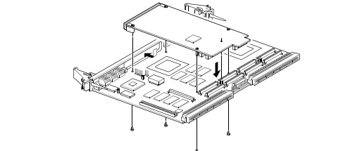
4. Line up the IPMC module’s front panel into the IPMC filler cutout slot on the host board’s front
panel.
5. Align connectors P11, P12, P13, P14, and P15 on the IPMC module with the mating connectors
on the host board and press firmly into place.
6. Insert the appropriate number of Phillips screws (typically 4) from the bottom of the host board
into the standoffs on the IPMC module and tighten the screws.
The host board is now ready to be installed into a VME chassis
Before You Install or Remove a Board
Boards may be damaged if improperly installed or handled. Please read and follow the
guidelines in this section to protect your equipment.
Observe ESD Precautions
Use ESD
Wrist Strap
ESD Emerson strongly recommends that you use an antistatic wrist strap and a conductive
foam pad when installing or upgrading a system. Electronic components, such as disk
drives, computer boards, and memory modules, can be extremely sensitive to
electrostatic discharge (ESD). After removing the component from its protective
wrapper or from the system, place the component flat on a grounded, static-free
surface (and, in the case of a board, component side up). Do not slide the component
over any surface.
If an ESD station is not available, you can avoid damage resulting from ESD by wearing
an antistatic wrist strap (available at electronics stores) that is attached to an active
electrical ground. Note that a system chassis may not be grounded if it is unplugged.
Watch for Bent Pins or Other Damage
!
Caution
Caution Bent pins or loose components can cause damage to the board, the backplane, or
other system components. Carefully inspect your board and the backplane for both pin
and component integrity before installation.
ECC and our suppliers take significant steps to ensure there are no bent pins on the backplane
or connector damage to the boards prior to leaving our factory. Bent pins caused by improper
installation or by boards with damaged connectors could void the warranty for the backplane or
boards.
If a system contains one or more crushed pins, power off the system and contact your local
sales representative to schedule delivery of a replacement chassis assembly.
Use Caution When Installing or Removing Boards
When first installing boards in an empty chassis, we recommend that you start at the left of the
card cage and work to the right when cards are vertically aligned; in horizontally aligned cages,
work from bottom to top.
When inserting or removing a board in a slot adjacent to other boards, use extra caution to avoid
damage to the pins and components located on the primary or secondary sides of the boards.
Preserve EMI Compliance
!
Caution
Caution To preserve compliance with applicable standards and regulations for electromagnetic
interference (EMI), during operation all front and rear openings on the chassis or board
faceplates must be filled with an appropriate card or covered with a filler panel. If the
EMI barrier is open, devices may cause or be susceptible to excessive interference.
Recognize Different Injector/Ejector Lever Types
The modules you install may have different ejector handles and latching mechanisms. The
following illustration shows the typical board ejector handles used with ECC payload cards: (A)
Elma Latching, (B) Rittal Type II, (C) Rittal Type IV. All handles are compliant with the
CompactPCI specification and are designed to meet the IEEE1101.10 standards.
Each lever type has a latching mechanism to prevent the lever from being opened accidentally.
You must press the lever release before you can open the lever. Never force the lever. If the lever
does not open easily, you may not have pressed firmly enough on the release. If the lever does
not close easily, the board may not be properly seated in the chassis.
To open a lever, press the release and move the lever outward away from the faceplate.
To close a lever, move the lever inward toward the faceplate until the latch engages.
Verify Slot Usage
!
Caution
Caution Prevent possible damage to module components by verifying the proper slot usage for
your configuration.
Figure 2-2. Injector/Ejector Lever Types
Programming
Programing Details
The overall design of the IPMC712 and IPMC761 is based on the PowerPlus II architecture. The
programming characteristics for both modules conforms to the PowerPlusII Programming
Specification.
Note The PowerPlus II Programming Specification covers a large variety of programming
configurations, many of which are not applicable to either module. This chapter describes those
aspects of the specification that are unique to both modules.
PCI Local Bus
The on-board PCI devices on the IPMC712 and the IPMC761 are the PCI-to-ISA Bridge and
the SCSI controller.
The PCI-to-ISA Bridge (PIB)
The PCI-to-ISA Bridge (PIB) provides the bridging functions between PCI local bus and the ISA
local resource bus. Other features contained in the PIB are:
■ 8259 Interrupt Controller
■ ISA DMA support
■ Timers and counters
The SCSI Controller
The SCSI controller’s clock speed is 40 MHz. The presence of the SCSI device can be positively
determined by reading the Device ID PCI Configuration Register 0x02 - 0x03. The Device ID is
0x0012.
The General Purpose I/O (GPIO) pin assignments for the SCSI Controller are shown in the
table below. A 1x4 switch (S1) is provided to configure GPIO pins 2 and 3. The factory default
setting shall be for Ultra-Speed and Ultra-Wide SCSI.
The General Purpose I/O (GPIO) pin assignments for the SCSI Controller are shown in the
table below. A 1x4 switch (S1) is provided to configure GPIO pins 2 and 3. The factory default
setting shall be for Ultra-Speed and Ultra-Wide SCSI.
SW1-P1 controls GPIO2 (Ultra/FAST SCSI) and SW1-P2 controls GPIO3 (Wide/Narrow SCSI
bus. SW1-P3 and SW1-P4 are No Connect. Select the SCSI characteristics of your
configuration according to the following table:
Table 3-1. GPIO Pin Assignments
GPIO Pin Direction Level Usage
GPIO1_MASTER_l output 1 SCSI LED; SCSI is not MASTER.
0 SCSI is MASTER.
GPIO2 input 1 SCSI speed; selectable by switch S1.
S1:1 OFF selects Ultra
0 S1:1 ON selects FAST (default).
GPIO3 input 1 SCSI bus width; selectable by switch S1.
S1:2 in OFF selects Wide-SCSI.
0 S1:2 in ON selects Narrow-SCSI.
0, 4, 5, 6, 7, 8 - - Not used
Table 3-2. SCSI Speed/Width Settings Using GPIO2:[1,2]
Figure 3-1. GPIO Switch Settings (S1)
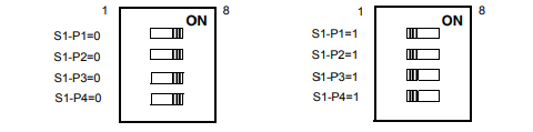
SW1-P1 controls GPIO2 (Ultra/FAST SCSI) and SW1-P2 controls GPIO3 (Wide/Narrow SCSI
bus. SW1-P3 and SW1-P4 are No Connect. Select the SCSI characteristics of your
configuration according to the following table:
Width of Bus Ultra (P1 OFF) Fast (P1 ON)
Wide (16-bit) SCSI bus (P2 OFF) 40MB/second 20MB/second
Narrow (8-bit) SCSI bus (P2 ON) 20MB/second 10MB/second
-
 Hirschmann RS20-1600M2T1SDAEHH03.1.02 Rail Switch
 -
 Hirschmann BRS30-24TX Industrial Rail Switch
 -
 Hirschmann RSPM20-4T14T1EV9HHS999.9.99 Managed Ethernet Switch
 -
 Hirschmann BELDEN RS40-0009CCCCSDAPHH09.0.14 / RS400009CCCCSDAPHH09014
 -
Hirschmann RS40 Rail Switch RS40-0009CCCCSDAE
-
 Hirschmann BELDEN RS30-0802T1T1SDAP / RS300802T1T1SDAP Fully Managed Layer 2 Compact Rail Switch
 -
 Hirschmann BELDEN RS20-0800M2M2SDAUHH / RS200800M2M2SDAUHH
 -
 Hirschmann EAGLE30-04022O6TT999SCCY9HSE3F Industrial Firewall Router Switch
 -
 Hirschmann RS20-1600T1T1SDAEHH09.0.14 RS20 Rail Mount Ethernet Switch
 -
 Hirschmann EAGLE0200T1T1TDDY90000HHE05.3.03 Industrial Security Router
 -
Hirschmann - BELDEN MIPP-AD-1L9P
-
 HIRSCHMANN RSPM20-4Z64Z6TV9HHS9 942 106-999 RAIL SAFETY SWITCH
 -
 HIRSCHMANN FIBEROPTIC MODULE FIP P/N: OZDFIPG3T
 -
 HIRSCHMANN RS20-1600M2M2SDAUHH Ethernet rack-mounted switch
 -
 HIRSCHMANN BELDEN RS20-0400T1T1SDAEHH04.0.01 / RS200400T1T1SDAEHH04001
 -
HIRSCHMANN MM2-4FXM3 MICE Media Module
-
HIRSCHMANN RS20-0800M2M2SDAE Industrial Ethernet Rail Switch
-
 Hirschmann RS20-2400T1T1SDAP / RS20-2400T1T1SDAPHH05.0.02
 -
 GE MLJ1005B010H00C MLJ Digital Synchromism Check
 -
 ALSTOM MICROTECH DX21-M2 Digital Excitation Controller
 -
HIRSCHMANN BRS20-1200ZZZZ-STCY99HHSES
-
 HIRSCHMANN MM3-4FXM2 MICE Media Module
 -
Hirschmann RSB20-0800T1T1SAABHH 8Port ENet Rail Switch RSB20
-
 Hirschmann MACH102-8TP Ethernet Switch
 -
 SAACKE DDZ-M marine steam pressure atomizer
 -
 SAACKE SKV-A marine rotary cup atomizer
 -
 SAACKE Seavis HMI05e
 -
 Kollmorgen MMC-SD-2.0-230 Servo Drive 100-240VAC 2KW 10A Output 3PH 100-240VAC
 -
 Kollmorgen Servo drive CR10550
 -
 Kollmorgen AKD-P01207-NACN-0054 Servo Driver
 -
 Kollmorgen S406M-CA-036 Servostar
 -
.png) Kollmorgen AKD-B02407-NAAN-0000 Digital Servo Drive
Kollmorgen AKD-B02407-NAAN-0000 Digital Servo Drive -
 Kollmorgen SERVOSTAR S406AM-CA Digital Servo Drive
 -
 KOLLMORGEN SERVOSTAR 603-AS SERVO AMPLIFIER_SERVOSTAR603AS_S60301
 -
Kollmorgen S700 Servo Controller (S70602-NANANA-NA)
-
 Kollmorgen MPK411 controller
 -
 KOLLMORGEN MMC-SD-1.3-460-D Smart Drive
 -
 KOLLMORGEN AKM21C-CKB2AA-00 / AKM21CCKB2AA00 Servomotor
 -
 BECKHOFF AX5106-0000-0200 | Digital Compact Servo Drives 1-channel
 -
 BECKHOFF C3620-0000 INDUSTRIAL COMPUTER (MOTORSHELVES)
 -
 Beckhoff EK1960-0000 TwinSAFE Compact Controller
 -
 Beckhoff C6930-0050 Control Cabinet Industrial PC
 -
 Beckhoff CP7711-0001-0030 Industrial Computer Detection
 -
 Beckhoff CX1001-0111 Embedded PC CPU Module
 -
 Beckhoff C6017-0020 | Ultra-compact Industrial PC
 -
 Beckhoff EK1322 | 2-port EtherCAT P junction with feed-in
 -
 Beckhoff CP2219-0010 Panel
 -
 BECKHOFF C6015-0020 ULTRA COMPACT INDUSTRIAL PC
 -
 BECKHOFF CX2030-0120/Standard CPU Module Embedded PC Windows PLC controller
 -
 Beckhoff CP7721-1090-0020 Panel PC
 -
 Beckhoff PC CPU Module CX5130-0175
 -
 Beckhoff C6920-0050 Control Cabinet
 -
 Beckhoff EL6631 EtherCAT 2-Port Communication Interface, Profinet RT Controller
 -
 Beckhoff CP6202-0001-0060 touch screen panel PC
 -
 Beckhoff CP3916-1002-0000 Multi-Touch Control Panel
 -
 Beckhoff EP1809-0021 | EtherCAT Box, 16-channel digital input, 24 V DC, 3 ms, M8Preferred type
 -
 Beckhoff CX8190 PLC Embedded Industrial PC Ethernet Controller
 -
 Beckhoff CX2100-0914 Power Supply for External
 -
 Beckhoff Automation CP6906-0001-0000 HMI
 -
 Beckhoff EP7342-0002 Module
 -
 Beckhoff CX1020-0112 / CX1100-0910 / CX1020-N010 / CX1100-0003 Windows CPU
 -
 Beckhoff EP7211-0034 EtherCAT Box 1 Channel Motion Interface
 -
 Beckhoff C6240-0030 Control cabinet Industrial PC
 -
 beckhoff motherboard CB1052-0004 CB1052-0004
 -
 Beckhoff AX2006-AS Servo Drive / Variable Frequency Drive
 -
BECKHOFF CP6207-0001-0020 NSMP
-
 Beckhoff C6930-1142-0060 Industrial Computer
 -
 Beckhoff FC7501-0000 interface card
 -
 Beckhoff CX5140-0175 Embedded PC PLC CPU CX5140 Industrial Controller
 -
 Beckhoff CP7802-1100-0010: High-End IP65 Control Panel with DVI/USB Extended Interface
 -
BECKHOFF CP3716-1058-0010 CONTROL PANEL
-
 Beckhoff AX8108-0000 Single-Axis Module
 -
 Beckhoff CU8851-0000 | USB extension, USB Extended 2.0 receiver box
 -
Beckhoff C6017-0030 | Ultra-compact Industrial PC
-
 Beckhoff CX1001-0120/CX10010120.cx1000-n001.cx1000-n000 System Overview
 -
 Beckhoff CPU Module CX5140-0155/4GB CPU Module
 -
 Beckhoff CP6533-0001-005: Built-in Panel PC with High-Definition Multi-Touch Control
 -
 Beckhoff EL5042 | EtherCAT Terminal, 2-channel encoder interface, BiSS® C
 -
 Beckhoff C6920-1080-0040: Premium Control Cabinet Industrial PC
 -
 Beckhoff C6920-0060 | Control cabinet Industrial PC
 -
 Beckhoff Embedded-PC CX5010-1121
 -
 Beckhoff CB3050-0010 Mainboard Motherboard
 -
 Beckhoff PLC module CX1020-0000 Basic CPU module (service phase)
 -
 Beckhoff CP7812-1056-0010 15" Multitouch Display Control Panel
 -
 Beckhoff CX5120-0115 /2GB Controller Module
 -
 Beckhoff CP7201-1000-0000 Industrial Panel PC
 -
 Beckhoff Servo Motor AM8061-0JH1-0000
 -
 BECKHOFF CP6503-0001-0050 Built-in Panel PC
 -
Beckhoff CP3919-0010 Display G190ETN01.2 19" PCT V04. Multi-touch Control Panel
-
 Beckhoff CX5110-0112-9020/000368201 Embedded PC Intel Atom Processor
 -
 Beckhoff AX8206-0000 Dual-Axis Module
 -
Beckhoff Nail Operating Terminal CP7032-1031-0010
-
Beckhoff AM8042-0EH1-0000 Servomotor 4.10 Nm (M0), F4 (87 mm)
-
 Beckhoff EK9300 Beckhoff CPU Module
 -
Beckhoff CP3224-0020 Multitouch-Panel-PC
-
 Beckhoff CP2712-0000 12.1" 24VDC Touch Screen WMD0
 -
 BECKHOFF CX5240-0195 / 0000289234 Embedded PC 40 GB CFast Card
 -
 Beckhoff CP6932-1000-0000 Control Panel
 -
 BECKHOFF CX5120-0121 PLC Module
 -
 Beckhoff EL3218 | EtherCAT Terminal, 8-channel analog input
 -
Beckhoff C6640-0050 | Control cabinet Industrial PC
-
 Beckhoff Cx5130-0120/4GB Embedded-PC
 -
 BECKHOFF CX2030-0122 PLC PROCESSOR
 -
 BECKHOFF CX5020-0122 Controller Module
 -
 Beckhoff CP3915-0000 Multitouch Panel
 -
 BECKHOFF EL3014 | EtherCAT Terminal
 -
 BECKHOFF Industrial Computer c6920-1057-0030
 -
 Beckhoff CX5130-0141/4GB CX5130-0141 Embedded PC
 -
 Beckhoff C6240-1052-0040 4-086-06-3073 Industrial Computer
 -
 Beckhoff CX5140-0135 /4GB High-Performance Embedded Industrial PC
 -
 Beckhoff C6515-1001-0000 Industrial PC
 -
 Beckhoff AX5103-0000-0200 - Digital Compact Servo Drives
 -
 Beckhoff CX2030-0130-1003/4GB Basic CPU module
 -
 Beckhoff AX8620-0000 Power Supply Module
 -
 Beckhoff CX9020-0111 module with
 -
 Beckhoff EL7332 PLC Module
 -
 BECKHOFF CP7709-0001-0020 HMI
 -
 Beckhoff CX5120-0155/2GB Embedded PC
 -
 BECKHOFF CP7037-1037-0010 OPERATOR INTERFACE TOUCHSCREEN
 -
 Beckhoff EK9000 | ModbusTCP/UDP Bus Coupler
 -
 Beckhoff Touch Panel Screen CP6020 -0000-0000
 -
 Beckhoff CX2020-0121 Module FAST Shipping
 -
 Beckhoff CX2030-0125 Basic CPU Module
 -
 Beckhoff CP3918-0000 Multi-Touch 18.5" Control Panel
 -
 Automotion LC4A00010 DC BL Motor Control, ATS, Sub Assy, SCP, 115VAC,
 -
 500T-115VAC - VAS ENGINEERING - DORIC 500 SERIES DIGITAL TEMP INDICATOR
 -
 Honeywell X-DCS2000/EN Digital Integrated System Manager 50/60Hz 100-240V #4
 -
 Kollmorgen S60600 Servostar600 606-Fan 4 kVA, 6 A, 3 X 230 - 480 V