EMERSONMVME55006E Single-Board Computer Installation and Use
in J3.
8. Insert the four screws (Phillips type) through the holes at the corners of
PMCspanx6E-010 and into the standoffs on the primary PMCspanx6E-002. Tighten
screws securely.
The screws have two different head diameters. Use the screws with the smaller
heads on the standoffs next to VMEbus connectors P1 and P2.
You are now ready to install the module into the VME chassis. Follow the procedure, Installing
the Board on page 33.
Installing the Board
Procedure
Use the following steps to install the MVME5500 into your computer chassis.
1. Attach an ESD strap to your wrist. Attach the other end of the ESD strap to an
electrical ground (refer to Unpacking Guidelines). The ESD strap must be secured
to your wrist and to ground throughout the procedure.
2. Remove any filler panel that might fill that slot.
3. Install the top and bottom edge of the MVME5500 into the guides of the chassis.
Only use injector handles for board insertion to avoid damage/deformation to the
front panel and/or PCB.
4. Ensure that the levers of the two injector/ejectors are in the outward position.
5. Slide the MVME5500 into the chassis until resistance is felt.
6. Simultaneously move the injector/ejector levers in an inward direction.
7. Verify that the MVME5500 is properly seated and secure it to the chassis using the
two screws located adjacent to the injector/ejector levers.
8. Connect the appropriate cables to the MVME5500.
1.9.1 Connection to Peripherals
When the MVME5500 is installed in a chassis, you are ready to connect peripherals and apply
power to the board.
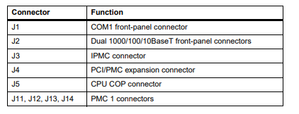
Figure 1-1 on page 20 shows the locations of the various connectors while Table 1-3 lists them
for you. Refer to Chapter 5, Connector Pin Assignments for the pin assignments of the
connectors listed below.
If a PMC module is plugged into PMC slot 1, the memory mezzanine card cannot be used
because the PMC module covers the memory mezzanine connector.
Figure 1-17 Installation into a Typical VME Chass

Completing the Installation
Verify that hardware is installed and the power/peripheral cables connected are appropriate for
your system configuration.
Replace the chassis or system cover, reconnect the system to the AC or DC power source, and
turn the equipment power on.
1.10 Startup and Operation
This section gives you information about:
z The power-up procedure
z Switches and indicators
1.11 Applying Power
After you verify that all necessary hardware preparation is complete and all connections are
made correctly, you can apply power to the system.
When you are ready to apply power to the MVME5500:
z Verify that the chassis power supply voltage setting matches the voltage present in the
country of use (if the power supply in your system is not auto-sensing)
z On powering up, the MVME5500 brings up the MotLoad prompt, MVME5500>
1.12 Switches and Indicators
The MVME5500 board provides a single push button switch that provides both Abort and Reset
(ABT/RST) functions. When the switch is depressed for less than three seconds, an abort
interrupt is generated to the processor. If the switch is held for more than three seconds, a
board hard reset is generated.
The MVME5500 has two front-panel indicators:
z BFL, software controlled. Asserted by firmware (or other software) to indicate a
configuration problem (or other failure).
z CPU, connected to a CPU bus control signal to indicate bus activity.
The following table describes these indicators:
Table 1-4 Front-Panel LED Status Indicators
Function Label Color Description
CPU Bus Activity CPU Green CPU bus is busy.
Board Fail BFL Yellow Board has a failure.
Functional Description
2.1 Overview
This chapter describes the MVME5500 on a block diagram level.
2.2 Block Diagram
Table 2-1 shows a block diagram of the overall board architecture.
Figure 2-1 Block Diagram

Features
The following table lists the features of the MVME5500.
Table 2-1 MVME5500 Features Summary

Processor
The MVME5500 supports the MPC7457 processor in the 483-pin CBGA package. The
processor consists of a processor core, an internal 256KB L2 and an internal L3 tag and
controller, which supports a backside L3 cache.
2.5 L3 Cache
The MVME5500 uses two 8Mb DDR synchronous SRAM devices for the processor’s L3 cache
data SRAM. This gives the processor a total of 2MB of L3 cache. These SRAM devices require
a 2.5V core voltage. The MVME5500 provides 1.5V as the SRAM I/O voltage. The L3 bus
operates at 200 MHz.
2.6 System Controller
The GT-64260B system controller for PowerPC architecture processors is a single chip solution
that provides the following features:
z A 64-bit interface to the CPU bus
z A 64-bit SDRAM interface
z A 32-bit generic device interface for Flash, etc.
z Two 64-bit, 66 MHz PCI bus interfaces
z Three 10/100Mb Ethernet MAC ports (two ports not used)
z A DMA engine for moving data between the buses
z An interrupt controller
z An I2C device controller
z PowerPC bus arbiter
z Counter/timers
-
 Hirschmann RS20-1600M2T1SDAEHH03.1.02 Rail Switch
 -
 Hirschmann BRS30-24TX Industrial Rail Switch
 -
 Hirschmann RSPM20-4T14T1EV9HHS999.9.99 Managed Ethernet Switch
 -
 Hirschmann BELDEN RS40-0009CCCCSDAPHH09.0.14 / RS400009CCCCSDAPHH09014
 -
Hirschmann RS40 Rail Switch RS40-0009CCCCSDAE
-
 Hirschmann BELDEN RS30-0802T1T1SDAP / RS300802T1T1SDAP Fully Managed Layer 2 Compact Rail Switch
 -
 Hirschmann BELDEN RS20-0800M2M2SDAUHH / RS200800M2M2SDAUHH
 -
 Hirschmann EAGLE30-04022O6TT999SCCY9HSE3F Industrial Firewall Router Switch
 -
 Hirschmann RS20-1600T1T1SDAEHH09.0.14 RS20 Rail Mount Ethernet Switch
 -
 Hirschmann EAGLE0200T1T1TDDY90000HHE05.3.03 Industrial Security Router
 -
Hirschmann - BELDEN MIPP-AD-1L9P
-
 HIRSCHMANN RSPM20-4Z64Z6TV9HHS9 942 106-999 RAIL SAFETY SWITCH
 -
 HIRSCHMANN FIBEROPTIC MODULE FIP P/N: OZDFIPG3T
 -
 HIRSCHMANN RS20-1600M2M2SDAUHH Ethernet rack-mounted switch
 -
 HIRSCHMANN BELDEN RS20-0400T1T1SDAEHH04.0.01 / RS200400T1T1SDAEHH04001
 -
HIRSCHMANN MM2-4FXM3 MICE Media Module
-
HIRSCHMANN RS20-0800M2M2SDAE Industrial Ethernet Rail Switch
-
 Hirschmann RS20-2400T1T1SDAP / RS20-2400T1T1SDAPHH05.0.02
 -
 GE MLJ1005B010H00C MLJ Digital Synchromism Check
 -
 ALSTOM MICROTECH DX21-M2 Digital Excitation Controller
 -
HIRSCHMANN BRS20-1200ZZZZ-STCY99HHSES
-
 HIRSCHMANN MM3-4FXM2 MICE Media Module
 -
Hirschmann RSB20-0800T1T1SAABHH 8Port ENet Rail Switch RSB20
-
 Hirschmann MACH102-8TP Ethernet Switch
 -
 SAACKE DDZ-M marine steam pressure atomizer
 -
 SAACKE SKV-A marine rotary cup atomizer
 -
 SAACKE Seavis HMI05e
 -
 Kollmorgen MMC-SD-2.0-230 Servo Drive 100-240VAC 2KW 10A Output 3PH 100-240VAC
 -
 Kollmorgen Servo drive CR10550
 -
 Kollmorgen AKD-P01207-NACN-0054 Servo Driver
 -
 Kollmorgen S406M-CA-036 Servostar
 -
.png) Kollmorgen AKD-B02407-NAAN-0000 Digital Servo Drive
Kollmorgen AKD-B02407-NAAN-0000 Digital Servo Drive -
 Kollmorgen SERVOSTAR S406AM-CA Digital Servo Drive
 -
 KOLLMORGEN SERVOSTAR 603-AS SERVO AMPLIFIER_SERVOSTAR603AS_S60301
 -
Kollmorgen S700 Servo Controller (S70602-NANANA-NA)
-
 Kollmorgen MPK411 controller
 -
 KOLLMORGEN MMC-SD-1.3-460-D Smart Drive
 -
 KOLLMORGEN AKM21C-CKB2AA-00 / AKM21CCKB2AA00 Servomotor
 -
 BECKHOFF AX5106-0000-0200 | Digital Compact Servo Drives 1-channel
 -
 BECKHOFF C3620-0000 INDUSTRIAL COMPUTER (MOTORSHELVES)
 -
 Beckhoff EK1960-0000 TwinSAFE Compact Controller
 -
 Beckhoff C6930-0050 Control Cabinet Industrial PC
 -
 Beckhoff CP7711-0001-0030 Industrial Computer Detection
 -
 Beckhoff CX1001-0111 Embedded PC CPU Module
 -
 Beckhoff C6017-0020 | Ultra-compact Industrial PC
 -
 Beckhoff EK1322 | 2-port EtherCAT P junction with feed-in
 -
 Beckhoff CP2219-0010 Panel
 -
 BECKHOFF C6015-0020 ULTRA COMPACT INDUSTRIAL PC
 -
 BECKHOFF CX2030-0120/Standard CPU Module Embedded PC Windows PLC controller
 -
 Beckhoff CP7721-1090-0020 Panel PC
 -
 Beckhoff PC CPU Module CX5130-0175
 -
 Beckhoff C6920-0050 Control Cabinet
 -
 Beckhoff EL6631 EtherCAT 2-Port Communication Interface, Profinet RT Controller
 -
 Beckhoff CP6202-0001-0060 touch screen panel PC
 -
 Beckhoff CP3916-1002-0000 Multi-Touch Control Panel
 -
 Beckhoff EP1809-0021 | EtherCAT Box, 16-channel digital input, 24 V DC, 3 ms, M8Preferred type
 -
 Beckhoff CX8190 PLC Embedded Industrial PC Ethernet Controller
 -
 Beckhoff CX2100-0914 Power Supply for External
 -
 Beckhoff Automation CP6906-0001-0000 HMI
 -
 Beckhoff EP7342-0002 Module
 -
 Beckhoff CX1020-0112 / CX1100-0910 / CX1020-N010 / CX1100-0003 Windows CPU
 -
 Beckhoff EP7211-0034 EtherCAT Box 1 Channel Motion Interface
 -
 Beckhoff C6240-0030 Control cabinet Industrial PC
 -
 beckhoff motherboard CB1052-0004 CB1052-0004
 -
 Beckhoff AX2006-AS Servo Drive / Variable Frequency Drive
 -
BECKHOFF CP6207-0001-0020 NSMP
-
 Beckhoff C6930-1142-0060 Industrial Computer
 -
 Beckhoff FC7501-0000 interface card
 -
 Beckhoff CX5140-0175 Embedded PC PLC CPU CX5140 Industrial Controller
 -
 Beckhoff CP7802-1100-0010: High-End IP65 Control Panel with DVI/USB Extended Interface
 -
BECKHOFF CP3716-1058-0010 CONTROL PANEL
-
 Beckhoff AX8108-0000 Single-Axis Module
 -
 Beckhoff CU8851-0000 | USB extension, USB Extended 2.0 receiver box
 -
Beckhoff C6017-0030 | Ultra-compact Industrial PC
-
 Beckhoff CX1001-0120/CX10010120.cx1000-n001.cx1000-n000 System Overview
 -
 Beckhoff CPU Module CX5140-0155/4GB CPU Module
 -
 Beckhoff CP6533-0001-005: Built-in Panel PC with High-Definition Multi-Touch Control
 -
 Beckhoff EL5042 | EtherCAT Terminal, 2-channel encoder interface, BiSS® C
 -
 Beckhoff C6920-1080-0040: Premium Control Cabinet Industrial PC
 -
 Beckhoff C6920-0060 | Control cabinet Industrial PC
 -
 Beckhoff Embedded-PC CX5010-1121
 -
 Beckhoff CB3050-0010 Mainboard Motherboard
 -
 Beckhoff PLC module CX1020-0000 Basic CPU module (service phase)
 -
 Beckhoff CP7812-1056-0010 15" Multitouch Display Control Panel
 -
 Beckhoff CX5120-0115 /2GB Controller Module
 -
 Beckhoff CP7201-1000-0000 Industrial Panel PC
 -
 Beckhoff Servo Motor AM8061-0JH1-0000
 -
 BECKHOFF CP6503-0001-0050 Built-in Panel PC
 -
Beckhoff CP3919-0010 Display G190ETN01.2 19" PCT V04. Multi-touch Control Panel
-
 Beckhoff CX5110-0112-9020/000368201 Embedded PC Intel Atom Processor
 -
 Beckhoff AX8206-0000 Dual-Axis Module
 -
Beckhoff Nail Operating Terminal CP7032-1031-0010
-
Beckhoff AM8042-0EH1-0000 Servomotor 4.10 Nm (M0), F4 (87 mm)
-
 Beckhoff EK9300 Beckhoff CPU Module
 -
Beckhoff CP3224-0020 Multitouch-Panel-PC
-
 Beckhoff CP2712-0000 12.1" 24VDC Touch Screen WMD0
 -
 BECKHOFF CX5240-0195 / 0000289234 Embedded PC 40 GB CFast Card
 -
 Beckhoff CP6932-1000-0000 Control Panel
 -
 BECKHOFF CX5120-0121 PLC Module
 -
 Beckhoff EL3218 | EtherCAT Terminal, 8-channel analog input
 -
Beckhoff C6640-0050 | Control cabinet Industrial PC
-
 Beckhoff Cx5130-0120/4GB Embedded-PC
 -
 BECKHOFF CX2030-0122 PLC PROCESSOR
 -
 BECKHOFF CX5020-0122 Controller Module
 -
 Beckhoff CP3915-0000 Multitouch Panel
 -
 BECKHOFF EL3014 | EtherCAT Terminal
 -
 BECKHOFF Industrial Computer c6920-1057-0030
 -
 Beckhoff CX5130-0141/4GB CX5130-0141 Embedded PC
 -
 Beckhoff C6240-1052-0040 4-086-06-3073 Industrial Computer
 -
 Beckhoff CX5140-0135 /4GB High-Performance Embedded Industrial PC
 -
 Beckhoff C6515-1001-0000 Industrial PC
 -
 Beckhoff AX5103-0000-0200 - Digital Compact Servo Drives
 -
 Beckhoff CX2030-0130-1003/4GB Basic CPU module
 -
 Beckhoff AX8620-0000 Power Supply Module
 -
 Beckhoff CX9020-0111 module with
 -
 Beckhoff EL7332 PLC Module
 -
 BECKHOFF CP7709-0001-0020 HMI
 -
 Beckhoff CX5120-0155/2GB Embedded PC
 -
 BECKHOFF CP7037-1037-0010 OPERATOR INTERFACE TOUCHSCREEN
 -
 Beckhoff EK9000 | ModbusTCP/UDP Bus Coupler
 -
 Beckhoff Touch Panel Screen CP6020 -0000-0000
 -
 Beckhoff CX2020-0121 Module FAST Shipping
 -
 Beckhoff CX2030-0125 Basic CPU Module
 -
 Beckhoff CP3918-0000 Multi-Touch 18.5" Control Panel
 -
 Automotion LC4A00010 DC BL Motor Control, ATS, Sub Assy, SCP, 115VAC,
 -
 500T-115VAC - VAS ENGINEERING - DORIC 500 SERIES DIGITAL TEMP INDICATOR
 -
 Honeywell X-DCS2000/EN Digital Integrated System Manager 50/60Hz 100-240V #4
 -
 Kollmorgen S60600 Servostar600 606-Fan 4 kVA, 6 A, 3 X 230 - 480 V