
EMERSONMVME55006E Single-Board Computer Installation and Use
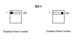
from being corrupted. The switch set to OFF disables all Flash 0 programming. The switch set
to ON enables the programming, this is the factory setting
Safe Start ENV Switch (S5-1)
This switch selects programmed or safe start ENV settings. When set to OFF, it indicates that
the programmed ENV settings should be used during boot. Set to ON indicates that the safe
ENV settings should be used.

Flash 0 Block Write Protect Switch (S3-2)
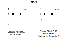
This switch supports the Intel J3 Flash family write protect feature. Set to OFF, it enables the
lock-down mechanism. Blocks locked down cannot be unlocked with the unlock command. The
switch must be set to ON in order to override the lock-down function and enable blocks to be
erased or programmed through software. Refer to the Intel J3 Flash data sheet, listed in
Appendix C, Related Documentation, for further details.
SROM Initialization Enable Switch (S5-2)
This switch enables/disables the GT-64260B SROM initialization. When set to 2, it enables the
GT-64260B device initialization via I2C SROM. Set to ON disables this initialization sequence

PCI Bus 0.0 Speed Switch (S4-1)
This switch can force PCI bus 0.0 to run at 33 MHz rather than the standard method of allowing
the PMC board to control whether the bus runs at 33 MHz or 66 MHz. Set to 1, it allows the
PMC board to choose the PCI 0.0 bus speed. Set to ON forces PCI bus 0.0 to run at 33 MHz

VME SCON Select Header (J27)
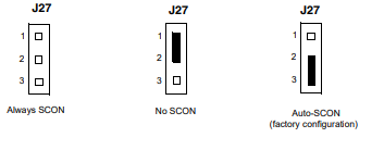
A 3-pin planar header allows the choice for auto/enable/disable SCON VME configuration. A
jumper installed across pins 1-2 configures for SCON disabled. A jumper installed across pins
2-3 configures for auto SCON. No jumper installed configures for SCON always enabled.
PCI Bus 1.0 Speed Switch (S4-2)
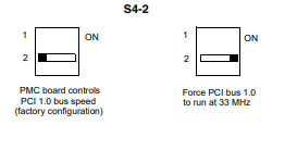
This switch can force PCI bus 1.0 to run at 33 MHz rather than the standard method of allowing
the PMC board to control whether the bus runs at 33 MHz or 66 MHz. Set to 1, it allows the
PMC board to choose the PCI 1.0 bus speed. Set to ON forces PCI bus 1.0 to run at 33 MHz
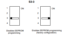
EEPROM Write Protect Switch (S3-3)
This switch enables/disables programming of the on-board EEPROMs as a means of protecting
the contents from being corrupted. Set to 1, it disables EEPROM programming by driving the
WP pin to a logic high. Set to ON to program any of the EEPROMs at addresses A0, A6, A8,
and/or AA.
Setting the PMC Vio Keying Pin
Signalling voltage (Vio) is determined by the location of the PMC Vio keying pin. Each site can
be independently configured for either +5V or +3.3V signalling. The option selected can be
determined by observing the location of the Vio keying pin.
Figure 1-13 S3-3 Settings
Disables EEPROM Enables EEPROM programming
programming (factory configuration)

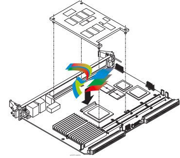
Installing the RAM5500 Module
Procedure
To upgrade or install a RAM5500 module, refer to and proceed as follows:
1. Attach an ESD strap to your wrist. Attach the other end of the ESD strap to the
chassis as a ground. The ESD strap must be secured to your wrist and to ground
throughout the procedure.
2. Perform an operating system shutdown. Turn the AC or DC power off and remove
the AC cord or DC power lines from the system. Remove the chassis or system
cover(s) as necessary for access to the VME boards.
3. Carefully remove the MVME5500 from its VME card slot and lay it flat, with
connectors P1 and P2 facing you.
4. Inspect the RAM5500 module that is being installed on the MVME5500 host board
to ensure that standoffs are installed in the four mounting holes on the module.
5. With standoffs installed in the four mounting holes on the RAM5500 module, align
the standoffs and the P1 connector on the module with the four holes and the P4
connector on the MVME5500 host board and press the two connectors together
until they are firmly seated in place.
7. Reinstall the MVME5500 assembly in its proper card slot following the procedure in
the next section. Be sure the host board is well seated in the backplane connectors.
Do not damage or bend connector pins.
8. Replace the chassis or system cover(s), reconnect the system to the AC or DC
power source and turn the equipment power on.
1.8 Installing PMCs
This section discusses the installation of a PMC module onto the MVME5500 and the
installation of a primary and secondary PMCspan module onto the PMC/MVME5500 processor
module.
If you have ordered one or more of the optional RAM500 memory mezzanine boards for the
MVME5500, ensure that they are installed on the board prior to proceeding. If they have not
been installed by the factory, and you are installing them yourself, please refer to Installing the
RAM5500 Module on page 28 for installation instructions. It is recommended that the memory
mezzanine modules be installed prior to installing other board accessories, such as PMCs,
IPMCs or transition modules.
1.8.1 Mounting the PMC Module
PMC modules mount on top of the MVME5500. Perform the following steps to install a
PMCmodule on your MVME5500.
Personal Injury or Death
Dangerous voltages, capable of causing death, are present in this equipment.


