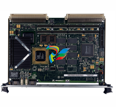
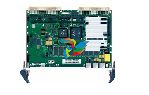
MOTOROLA MVME162-10 Embedded Controller
MOTOROLA MVME162-10 Embedded Controller
Related Documentation
The following publications are applicable to the MVME162 and may provide
additional helpful information. If not shipped with this product, they may be
purchased by contacting your local Motorola sales office. Non-Motorola
documents may be purchased from the sources listed
The following publications are available from the sources indicated.
Versatile Backplane Bus: VMEbus, ANSI/IEEE Std 1014-1987. The Institute of
Electrical and Electronics Engineers, Inc., 345 East 47th Street, New York, NY
10017 (VMEbus Specification). This is also available as Microprocessor system
bus for 1 to 4 byte data, IEC 821 BUS, Bureau Central de la Commission
Electrotechnique Internationale; 3. rue de Varembé, Geneva, Switzerland.
ANSI Small Computer System Interface-2 (SCSI-2), Draft Document X3.131-198X,
Revision 10c; Global Engineering Documents, P.O. Box 19539. Irvine, CA 92714.
IndustryPack Logic Interface Specification, Revision 1.0; GreenSpring Computers,
Inc., 1204 O’Brien Drive, Menlo Park, CA 94025.
82596CA Local Area Network Coprocessor data sheet, order number 290218; and
82596 User’s Manual, order number 296853; Intel Corporation, Literature
Sales, P.O. Box 58130. Santa Clara, CA 95052-8130.
NCR 53C710 SCSI I/O Processor Data Manual, order number NCR53C710DM;
and NCR 53C710 SCSI I/O Processor Programmer’s Guide, order number
NCR53C710PG; NCR Corporation, Microelectronics Products Division,
Colorado Springs, CO.
MK48T08(B) Timekeeper™ and 8Kx8 Zeropower™ RAM data sheet in Static
RAMs Databook, Order Code DBSRAM71; SGS-THOMPSON Microelectronics
Group; North & South American Marketing Headquarters, 1000 East Bell
Road, Phoenix, AZ 85022-2699.
Z85230 Serial Communications Controller data sheet, Zilog Inc., 210 Hacienda
Ave., Campbell, CA 95008-6609.
28F008SA Flash Memory Data Sheet, Order Number 290435-001; Intel Literature
Sales, P.O. Box 7641. Mt. Prospect, IL 60056-7641.
28F020 Flash Memory Data Sheet, Order Number 290245-003; Intel Literature
Sales, P.O. Box 7641. Mt. Prospect, IL 60056-7641.
Support Information
You can obtain connector interconnect signal information, parts lists, and
schematics for the MVME162 free of charge by contacting your local Motorola
sales office
Manual Terminology
Throughout this manual, a convention is used which precedes data and
address parameters by a character identifying the numeric format as follows:
$
dollar
% percent
specifies a hexadecimal character
specifies a binary number
& ampersand specifies a decimal number
Unless otherwise specified, all address references are in hexadecimal.
An asterisk (*) following the signal name for signals which are level-significant
denotes that the signal is true or valid when the signal is low.
An asterisk (*) following the signal name for signals which are edge-significant
denotes that the actions initiated by that signal occur on high-to-low
transition.
In this manual, assertion and negation are used to specify forcing a signal to a
particular state. In particular, assertion and assert refer to a signal that is active
or true; negation and negate indicate a signal that is inactive or false. These
terms are used independently of the voltage level (high or low) that they
represent.
In this manual, MVME712 series transition module refers generically to the
MVME712-12. MVME712-13. MVME712A, MVME712AM, or MVME712M.
MVME712x transition module refers to the closely related MVME712-12.
MVME712-13. MVME712A, or MVME712AM (not to the MVME712M).
References to a specific module use the complete designation of that module.
Data and address sizes are defined as follows:
A byte is eight bits, numbered 0 through 7. with bit 0 being the least
significant.
A word is 16 bits, numbered 0 through 15. with bit 0 being the least
significant.
A longword is 32 bits, numbered 0 through 31. with bit 0 being the least
significant
Introduction
This chapter provides unpacking instructions, hardware preparation
guidelines, and installation instructions for the MVME162 Embedded
Controller. Hardware preparation for the MVME712 series transition
modules is described in separate manuals; refer to the Related Documentation
section in Chapter 1
Hardware Preparation
To produce the desired configuration and ensure proper operation of the
MVME162. you may need to carry out certain modifications before installing
the module.
The MVME162 provides software control over most options: by setting bits in
control registers after installing the MVME162 in a system, you can modify its
configuration. (The MVME162 registers are described in Chapter 4. and/or in
the MVME162 Embedded Controller Programmer’s Reference Guide as listed in
Related Documentation in Chapter 1.)
Some options, however, are not software-programmable. Such options are
controlled by manual installation or removal of header jumpers or interface
modules
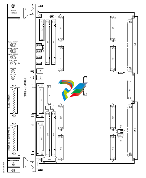
Figure 2-1 illustrates the placement of the switches, jumper headers,
connectors, and LED indicators on the MVME162. Manually configurable
items include:
SIM selection for serial port B configuration (J10)
System controller selection (J1)
Synchronous clock selection (J11) for Serial Port 1/Console
Synchronous clock selection (J12) for Serial Port 2
SRAM backup power source selection (J20)
EPROM size selection (J21)
General-purpose readable register configuration (J22)
The MVME162 has been factory tested and is shipped with the configurations
described in the following sections. The MVME162’s required and factory
installed Debug Monitor, MVME162Bug (162Bug), operates with those factory
settings.
SIM Selection
Port B of the MVME162’s Z85230 serial communications controller is
configurable via a serial interface module (SIM) which is installed at connector
J10 on the MVME162 board. Four serial interface modules are available:
EIA-232-D (DCE and DTE)
EIA-530 (DCE and DTE)
You can change Port B from an EIA-232-D to an EIA-530 interface (or vice
versa) by mounting the appropriate serial interface module. Port B is routed
(via the SIM at J10) to the 25-pin DB25 front panel connector marked SERIAL
PORT 2.
For the location of SIM connector J10 on the MVME162. refer to Figure 2-1.
Figure 2-2 illustrates the secondary side (bottom) of a serial interface module,
showing the J1 connector which plugs into SIM connector J10 on the
MVME162. Figure 2-3 (sheets 3-6), Figure 2-4 (sheets 3-4), and Figure 2-5
illustrate the configurations available for Port B.
For the part numbers of the serial interface modules, refer to Table 2-1. The
part numbers are ordinarily printed on the primary side (top) of the SIMs, but
may be found on the secondary side in some versions.
If you need to replace an existing serial interface module with a SIM of another
type, go to Removal of Existing SIM below. If there is no SIM on the main board,
skip to Installation of New SIM.
| User name | Member Level | Quantity | Specification | Purchase Date |
|---|


-
 Hirschmann Industrial Ethernet Rail Switch RS20 Basic Family
 -
 GE Grid Solutions P40U Px40 USB Adaptor
 -
 ABB ontinuous Gas Analyzers AO2000 Series AO2040CU Ex Central Unit in Category 2G
 -
 ABB Advance Optima AO2000 Series Continuous gas analyzers Models AO2020. AO2040
 -
 Advance Optima Module Uras 14
 -
 SAACKE control optimization
 -
 SAACKE se@vis efficiency monitor
 -
 SAACKE se@vis pro
 -
 SAACKE se@vis eco
 -
 SAACKE se@vis compact
 -
 HIRSCHMANN Industrial ETHERNET Switch MICE MS20/MS30
 -
 HIRSCHMANN MICE Media modules
 -
 Kongsberg GL-10 Level Switch
 -
 B&R ACOPOSinverter P74 frequency converter
 -
 Beckhoff CX2020 | Basic CPU module (service phase)
 -
 Beckhoff CX1010 | Basic CPU module (service phase)
 -
 Beckhoff CX5120 | Embedded PC with Intel Atom® E3815
 -
 Beckhoff CP69xx-xxxx-0010 | Economy built-in Control Panel with DVI/USB Extended interface
 -
 Beckhoff CP29xx-0000 | Multi-touch built-in Control Panel with DVI/USB Extended interface
 -
 SAACKE Monoblock Rotary Cup Burner SKVJ-M
 -
 ABB Plantguard Fault Tolerant Technology Architecture and Software
 -
 OMRON H8PR-8/H8PR-8P H8PR-16/H8PR-16P H8PR-24/H8PR-24P Rotary Positioner
 -
 ABB PFSA107-Z42 DTU Stressometer Digital Transmission Unit
 -
 Nidec Mentor MP
 -
 IBA ibaNet-E
 -
 IBA FO Connection to Reflective Memory
 -
 IBA FO Connection to Siemens Systems
 -
 IBA Interface Cards For Fiber Optic Connections
 -
 IBA Field and Drive Buses
 -
 IBA ibaPADU-S Modular System
 -
 IBA ibaMAQS
 -
 STUCKE SYMAP®ARC
 -
 STUCKE SYMAP®R
 -
 STUCKE SYMAP®Compact
 -
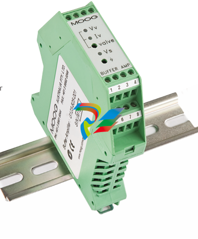 MOOG G123-825-001 BUFFER AMPLIFIER
 -
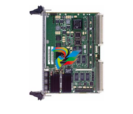 Motorola MVME5100 Series VME Processor Modules
 -
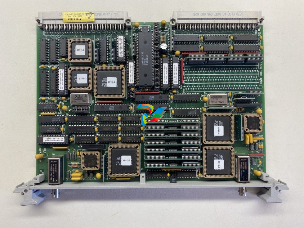
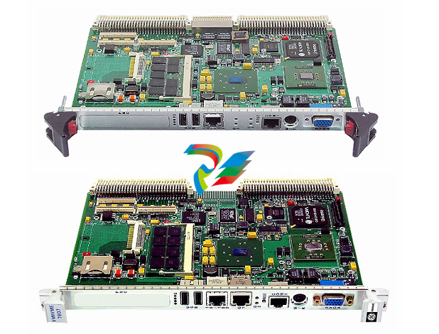
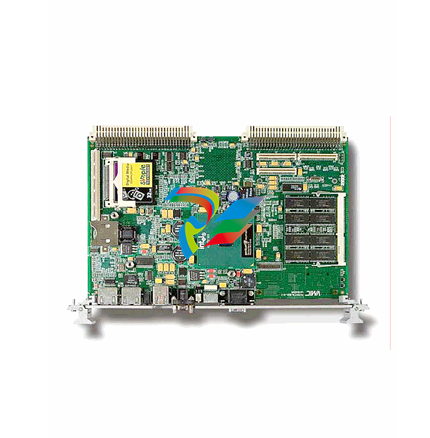
 Motorola MVME162 Embedded Controller
 -
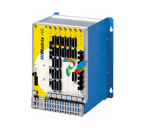 HIMatrix Safety-Related Controller System Manual for the Modular Systems
 -
 Motorola MVME2400 Series VME Processor Module
 -
 Sieger System 57
 -
 KONGSBERG MRU product line continuation
 -
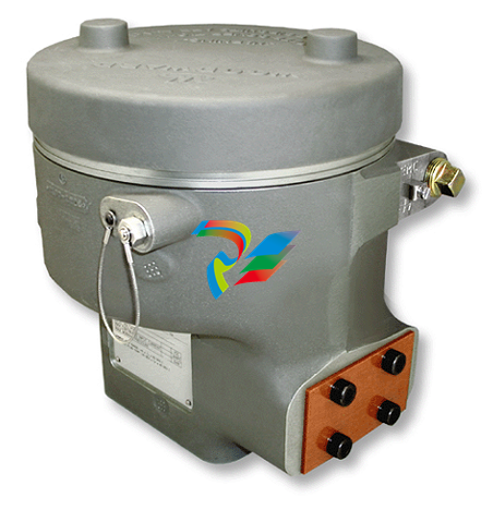
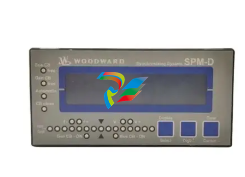
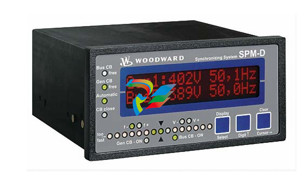
 Woodward easYgen-3100/3200 Genset Control for Multiple Unit Operation
 -
 Woodward MFR 300 Multifunction Relay / Measuring
 -
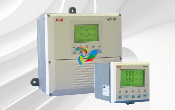 ABB AX410, AX411, AX413, AX416, AX418, AX450, AX455 and AX456 Single and dual input analyzers for low level conductivity
 -
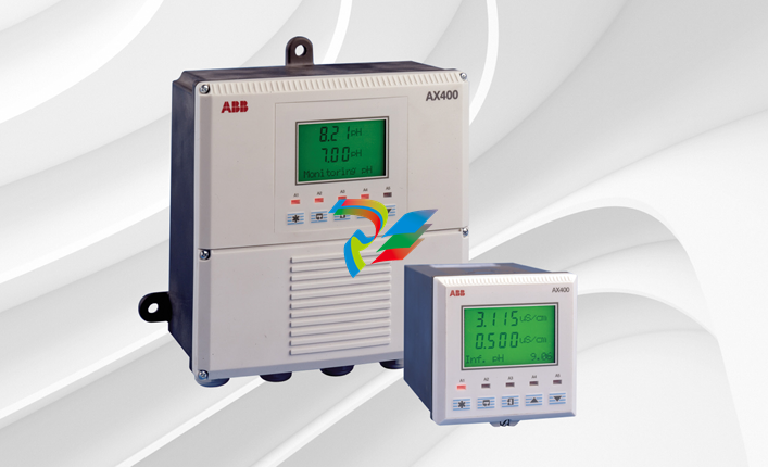 ABB AX410, AX411, AX416, AX450 and AX455 Single and dual input analyzers
 -
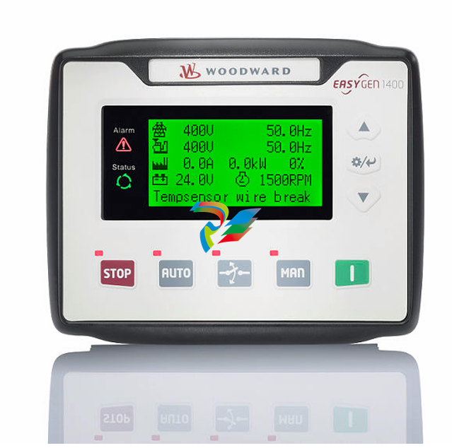 Woodward easYgen-1400 Technical Manual Genset Control
 -
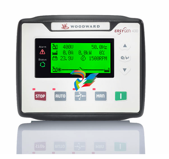 Woodward easYgen-400 Operation Manual Genset Control
 -
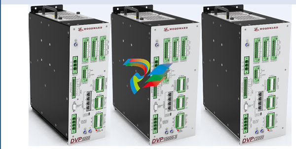 Woodward High Output Digital Valve Positioner (DVP)DVP5000/DVP10000/DVP12000
 -
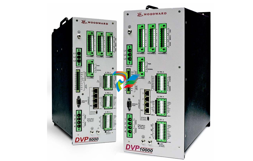 Woodward High Output Digital Valve Positioner DVP5000 and DVP10000
 -
 Woodward TG611-13/-17 Overspeed Test Device Conversion Kit
 -
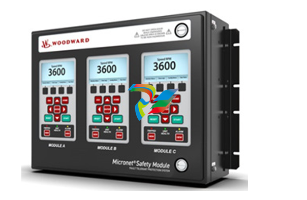 Woodward MicroNet Safety Module (MSM)
 -
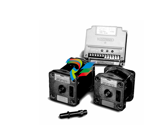
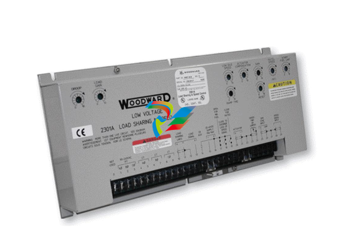 Woodward 2301A Electronic Load Sharing and Speed Control 9905/9907 Series
 -
 Woodward-Service Bulletin 01671
 -
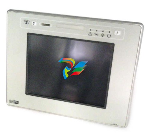
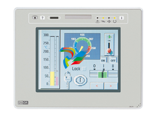
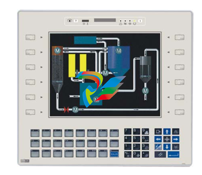
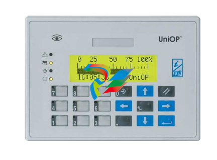
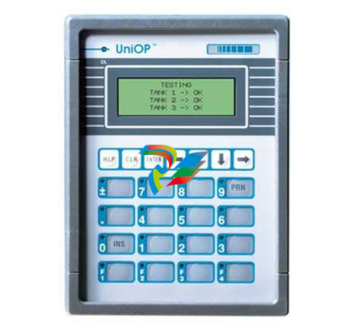
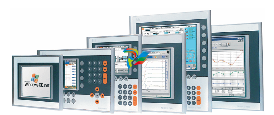
 UniOP eTOP40B 12.1” TFT color display
 -
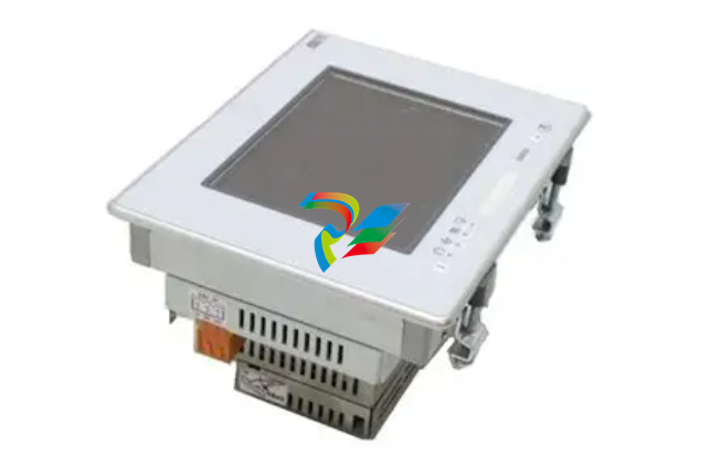
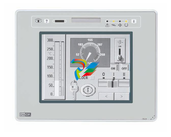
 UniOP eTOP40 TFT Color display
 -
 UniOP eTOP33B 10.4” TFT color display
 -
 UniOP eTOP33C eTOP33-0050 Resistive touchscreen
 -
UniOP eTOP30. eTOP32 eTOP32-0050 Human-machine interface equipment
-
 UniOP eTOP20B and eTOP21B eTOP20B-0050
 -
 UniOP eTOP12 eTOP12-0050 Advanced human-machine interface equipment
 -
 UniOP eTOP11 eTOP11-0050 HMI
 -
 UniOP eTOP06C HMI
 -
 UniOP eTOP06 HMI
 -
 UniOP eTOP05EB eTOP05EB-DF45 HMI
 -
 UniOP eTOP05. eTOP05P Human-machine interface equipment
 -
 UniOP eTOP03 eTOP03-0046
 -
 UniOP eTOP507 507U2P1 eTOP Series 500 Human-Machine Interface
 -
 UniOP eTOP307
 -
 UniOP ETT-VGA Human-machine interface touch unit
 -
 UniOP ePAD32B, ePAD33B and ePAD33BT ePAD33B-0350
 -
 UniOP ePAD05 and ePAD06
 -
 UniOP CP02R-04 Human-machine interface
 -
 UniOP ERT-16 - Industrial PLC Workstation
 -
 UniOP ePAD03 and ePAD04
 -
 UNIOP EPALM10-DA71 state-of-the-art handheld HMI
 -
 Watlow SERIES CLS200 SPECIFICATION SHEET
 -
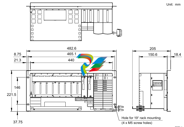
 Detailed Explanation of B&R Power Panel 300/400: The Core of Industrial Automation Control
 -
 YOKOGAWA Models ANB10S, ANB10D, ANR10S, ANR10D Node Units (for FIO)
 -
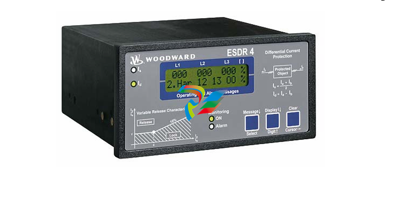 Woodward ESDR 4 Current Differential Protection Relay
 -
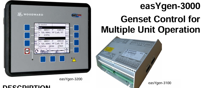 Woodward easYgen-3000 Genset Control for
 -
 Woodward CPC-II Current-to-Pressure Converter
 -
 Woodward 8290-189-EPG-installation-manual 8290-044
 -
 Woodward Product Change Notification 06946A
 -
 Woodward Product Change Notification 06912
 -
 Fisher™ 4660 High-Low Pressure Pilot
 -
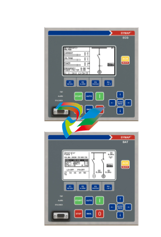 Flexible digital protection and control equipment SYMAP®
 -
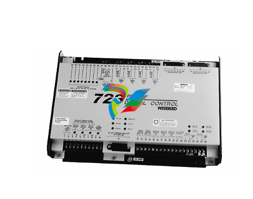 Woodward 723PLUS Digital Control
 -
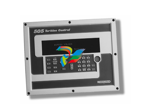
 Woodward 505 Digital Controller For steam turbineses
 -
 Woodward 85018V2 505E Digital Governor for Extraction Steam Turbines
 -
Woodward 85018V1 Turbine Control Parameters
-
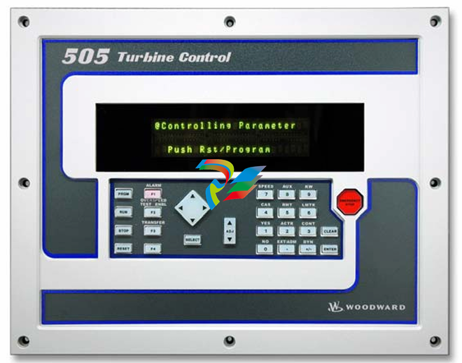
Woodward 26871 505 Enhanced Digital Control for Steam Turbines
-
 Woodward 03365 505E (Extraction / Admission)
 -
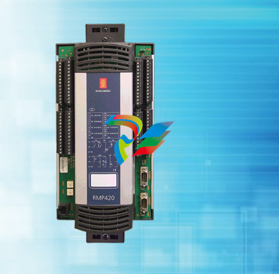 KONGSBERG RMP420-Remote Multipurpose Input/Output
 -
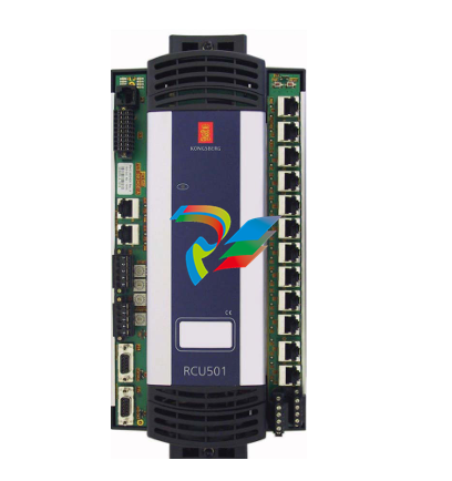 KONGSBERG RCU501 Remote Controller Unit
 -
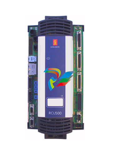 KONGSBERG RCU500 Remote Controller Unit
 -
 K-Gauge TOP KONGSBERG Tank Overfill Protection SystemFeatures
 -
 Kongsberg DPS112 DGNSS (DGPS/DGLONASS) sensor
 -
 Kongsberg d0000930-presafe-atex-report signed
 -
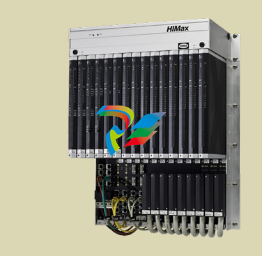 HIMax TECHNICAL FACTS X Series
 -
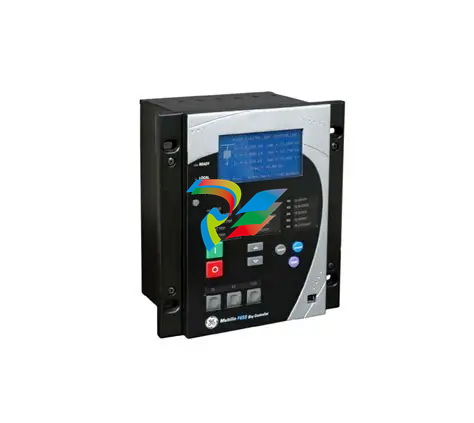 GE Multilin F650
 -
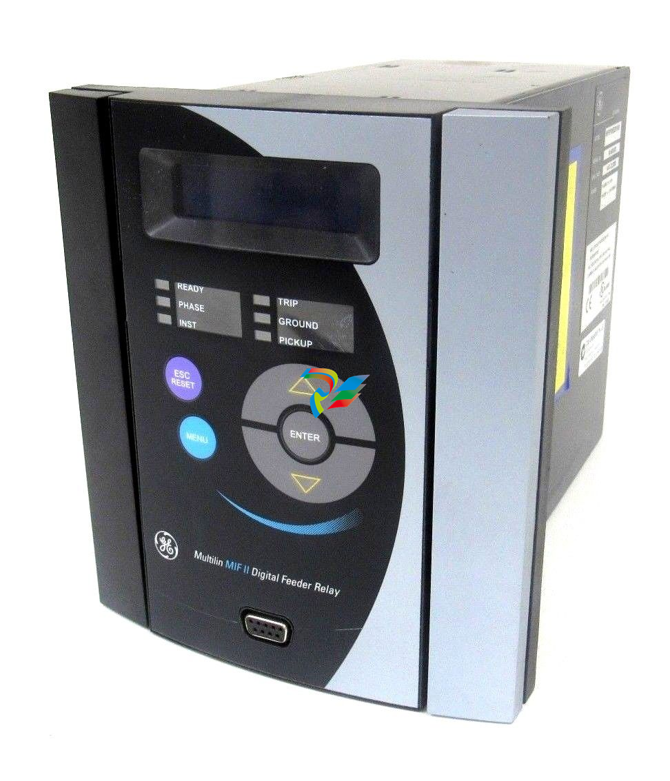 GE MIF II - Legacy
 -
 GE PQM II Power QualIty Meter
 -
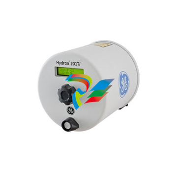 Hydran 201Ti Mark IV Essential DGA monitoring for transformers
 -
 alstom AMS42/84 5B Amplifier SystemAmplifier Technology at its Best.
 -
 GE VMIVME-5576 Fiber-Optic Reflective Memory with Interrupts
 -
 GE Multilin 750/760 - Legacy Feeder Protection System
 -
 GE Fanuc Automation VMICPCI-7806 Specifications
 -
 VMIVME-7807 VME-7807RC* Intel® Pentium® M-Based VME SBC
 -
 GE Fanuc Automation VMIVME-7750 Specifications
 -
 FOXBORO Compact FBM240. Redundant with Readback, Discrete
 -
 FOXBORO FBM208/b, Redundant with Readback, 0 to 20 mA I/O Module
 -
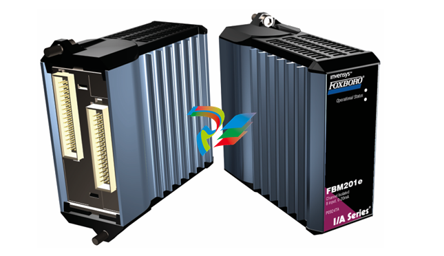 FOXBORO FBM201e Analog Input (0 to 20 mA) Interface Modules
 -
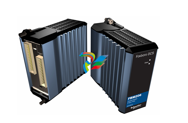 Foxboro DCS FBM206 Pulse Input Module
 -
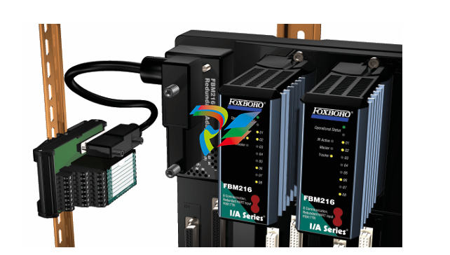 FOXBORO FBM216 HART® Communication Redundant Input Interface Module
 -
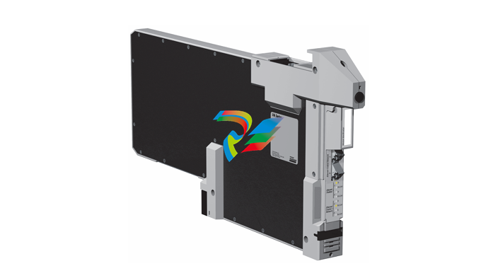 FOXBORO Z-Module Control Processor 270 (ZCP270)
 -
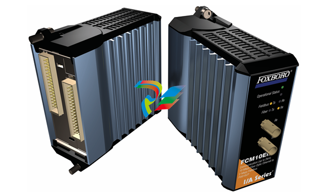 FOXBORO Fieldbus Communications Module, FCM10Ef
 -
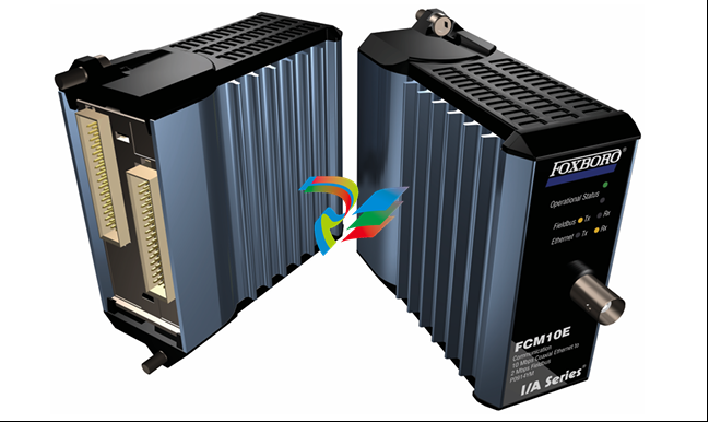 FOXBORO Fieldbus Communications Module, FCM10E
 -
 Foxboro DCS Compact FBM241/c/d, Redundant, Discrete I/O Modules
 -
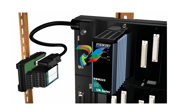
Foxboro FBM223 PROFIBUS-DP™ Communication Interface Module
-
 Foxboro DCS FBM204. 0 to 20 mAI/OModule
 -
Foxboro FBM239, Discrete 16DI/16DO Module
-
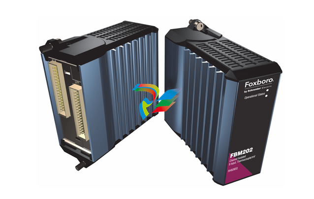
Foxboro FBM202 Thermocouple/mV Input Module
-
 Foxboro E69F Current-to-Pneumatic Signal Converter
 -
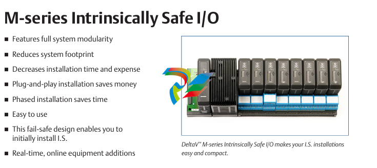 EMERSON M-series Intrinsically Safe I/O
 -
 MVME6100 Series VMEbus Single-Board Computer
 -
 Configuration for AMS 6500 Protection Monitors
 -
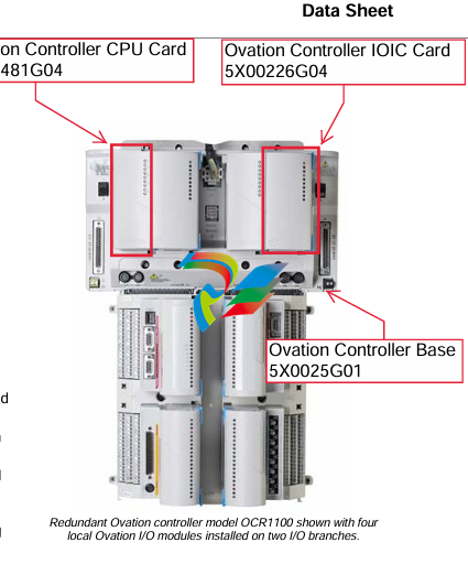 Ovation™ Controller Model OCR1100 (5X00481G04/5X00226G04)
 -
 ABB UCU-22, UCU-23 andUCU-24control units