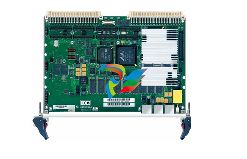
MOTOROLA MVME162-210 Embedded Controller
The MK48T08 BBRAM (also called Non-Volatile RAM or NVRAM) is divided
into six areas as shown in Table 3-10. The first five areas are defined by
software, while the sixth area, the time-of-day (TOD) clock, is defined by the
chip hardware. The first area is reserved for user data. The second area is used
by Motorola networking software. The third area is used by the operating
system. The fourth area is used by the MVME162 board debugger
(MVME162Bug). The fifth area, detailed in Table 3-11. is the configuration
area. The sixth area, the TOD clock, detailed in Table 3-12. is defined by the
chip hardware.
The data structure of the configuration bytes starts at $FFFC1EF8 and is as
follows.
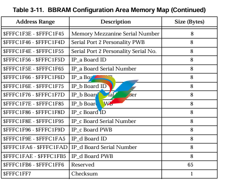
The fields are defined as follows:
1. Four bytes are reserved for the revision or version of this structure. This
revision is stored in ASCII format, with the first two bytes being the major
version numbers and the last two bytes being the minor version numbers.
For example, if the version of this structure is 1.0. this field contains:
0100
2. Twelve bytes are reserved for the serial number of the board in ASCII
format. For example, this field could contain:
000000470476
3. Sixteen bytes are reserved for the board ID in ASCII format. For example,
for an MVME162 board with MC68040. SCSI, Ethernet, 4MB DRAM, and
512KB SRAM, this field contains:
MVME162-23 (The 10 characters are followed by six blanks.)
4. Sixteen bytes are reserved for the printed wiring assembly (PWA) number
assigned to this board in ASCII format. This includes the 01-W prefix. This
is for the main logic board if more than one board is required for a set.
Additional boards in a set are defined by a structure for that set. For
example, for an MVME162 board with MC68040. SCSI, Ethernet, 4MB
DRAM, and 512KB SRAM, at revision A, the PWA field contains:
01-W3814B01A (The 12 characters are followed by four blanks.)
5. Four bytes contain the speed of the board in MHz. The first two bytes are
the whole number of MHz and the second two bytes are fractions of MHz.
For example, for a 25.00 MHz board, this field contains:
2500
6. Six bytes are reserved for the Ethernet address. The address is stored in
hexadecimal format. (Refer to the detailed description in Chapter 4.) If the
board does not support Ethernet, this field is filled with zeros.
7. These two bytes are reserved.
8. Two bytes are reserved for the local SCSI ID. The SCSI ID is stored in
ASCII format.
9. Eight bytes are reserved for the printed wiring board (PWB) number
assigned to the memory mezzanine board in ASCII format. This does not
include the 01-W prefix. For example, for a 4MB parity mezzanine at
revision A, the PWB field contains:
3837B02A
10. Eight bytes are reserved for the serial number assigned to the memory
mezzanine board in ASCII format
Eight bytes are reserved for the printed wiring board (PWB) number
assigned to the serial port 2 personality board in ASCII format.
12. Eight bytes are reserved for the serial number assigned to the serial port 2
personality board in ASCII format.
13. Eight bytes are reserved for the board identifier, in ASCII format, assigned
to the optional first IndustryPack a.
14. Eight bytes are reserved for the serial number, in ASCII format, assigned
to the optional first IndustryPack a.
15. Eight bytes are reserved for the printed wiring board (PWB) number
assigned to the optional first IndustryPack a.
16. Eight bytes are reserved for the board identifier, in ASCII format, assigned
to the optional second IndustryPack b.
17. Eight bytes are reserved for the serial number, in ASCII format, assigned
to the optional second IndustryPack b.
18. Eight bytes are reserved for the printed wiring board (PWB) number
assigned to the optional second IndustryPack b.
19. Eight bytes are reserved for the board identifier, in ASCII format, assigned
to the optional third IndustryPack c.
20. Eight bytes are reserved for the serial number, in ASCII format, assigned
to the optional third IndustryPack c.
21. Eight bytes are reserved for the printed wiring board (PWB) number
assigned to the optional third IndustryPack c.
22. Eight bytes are reserved for the board identifier, in ASCII format, assigned
to the optional fourth IndustryPack d.
23. Eight bytes are reserved for the serial number, in ASCII format, assigned
to the optional fourth IndustryPack d.
24. Eight bytes are reserved for the printed wiring board (PWB) number
assigned to the optional fourth IndustryPack d.
25. Growth space (65 bytes) is reserved. This pads the structure to an even 256
bytes.
26. The final one byte of the area is reserved for a checksum (as defined in the
MVME162Bug Debugging Package User’s Manual) for security and data
integrity of the configuration area of the NVRAM. This data is stored in
hexadecimal format.
| NI | NI-9505 |
| NI | PXI-4071 |
| NI | CFP-AI-111 |
| NI | FP-TB-1 |
| NI | PXI-6527 |
| NI | SCXI-1140 |
| NI | PXI-4462 |
| NI | PXI-6608 |
| NI | PXI-4461 |
| NI | PXI-4351 |
| NI | SCXI-1102B |
| NI | SCXI-1121 |
| NI | CFP-CB-1 |
| NI | CFP-DO-403 |
| NI | CFP-DI-304 |
| NI | CFP-DO-400 |
| User name | Member Level | Quantity | Specification | Purchase Date |
|---|


-
 Hirschmann Industrial Ethernet Rail Switch RS20 Basic Family
 -
 GE Grid Solutions P40U Px40 USB Adaptor
 -
 ABB ontinuous Gas Analyzers AO2000 Series AO2040CU Ex Central Unit in Category 2G
 -
 ABB Advance Optima AO2000 Series Continuous gas analyzers Models AO2020. AO2040
 -
 Advance Optima Module Uras 14
 -
 SAACKE control optimization
 -
 SAACKE se@vis efficiency monitor
 -
 SAACKE se@vis pro
 -
 SAACKE se@vis eco
 -
 SAACKE se@vis compact
 -
 HIRSCHMANN Industrial ETHERNET Switch MICE MS20/MS30
 -
 HIRSCHMANN MICE Media modules
 -
 Kongsberg GL-10 Level Switch
 -
 B&R ACOPOSinverter P74 frequency converter
 -
 Beckhoff CX2020 | Basic CPU module (service phase)
 -
 Beckhoff CX1010 | Basic CPU module (service phase)
 -
 Beckhoff CX5120 | Embedded PC with Intel Atom® E3815
 -
 Beckhoff CP69xx-xxxx-0010 | Economy built-in Control Panel with DVI/USB Extended interface
 -
 Beckhoff CP29xx-0000 | Multi-touch built-in Control Panel with DVI/USB Extended interface
 -
 SAACKE Monoblock Rotary Cup Burner SKVJ-M
 -
 ABB Plantguard Fault Tolerant Technology Architecture and Software
 -
 OMRON H8PR-8/H8PR-8P H8PR-16/H8PR-16P H8PR-24/H8PR-24P Rotary Positioner
 -
 ABB PFSA107-Z42 DTU Stressometer Digital Transmission Unit
 -
 Nidec Mentor MP
 -
 IBA ibaNet-E
 -
 IBA FO Connection to Reflective Memory
 -
 IBA FO Connection to Siemens Systems
 -
 IBA Interface Cards For Fiber Optic Connections
 -
 IBA Field and Drive Buses
 -
 IBA ibaPADU-S Modular System
 -
 IBA ibaMAQS
 -
 STUCKE SYMAP®ARC
 -
 STUCKE SYMAP®R
 -
 STUCKE SYMAP®Compact
 -
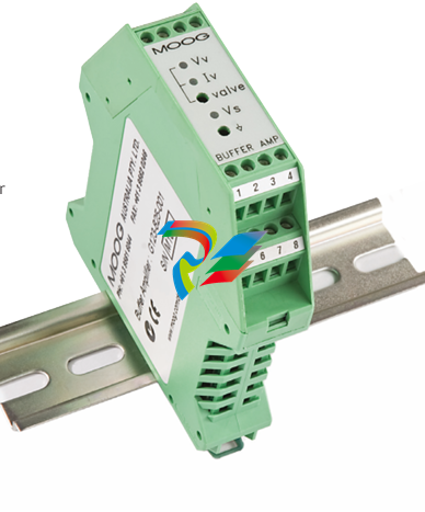 MOOG G123-825-001 BUFFER AMPLIFIER
 -
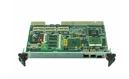
 Motorola MVME5100 Series VME Processor Modules
 -
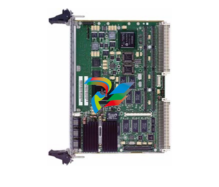
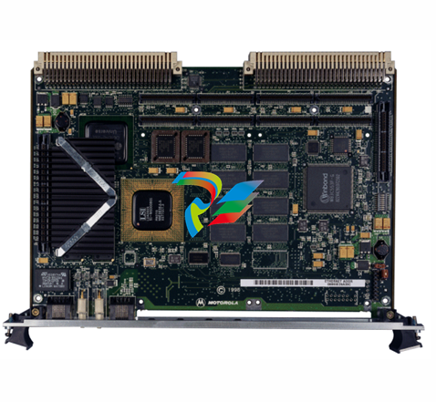
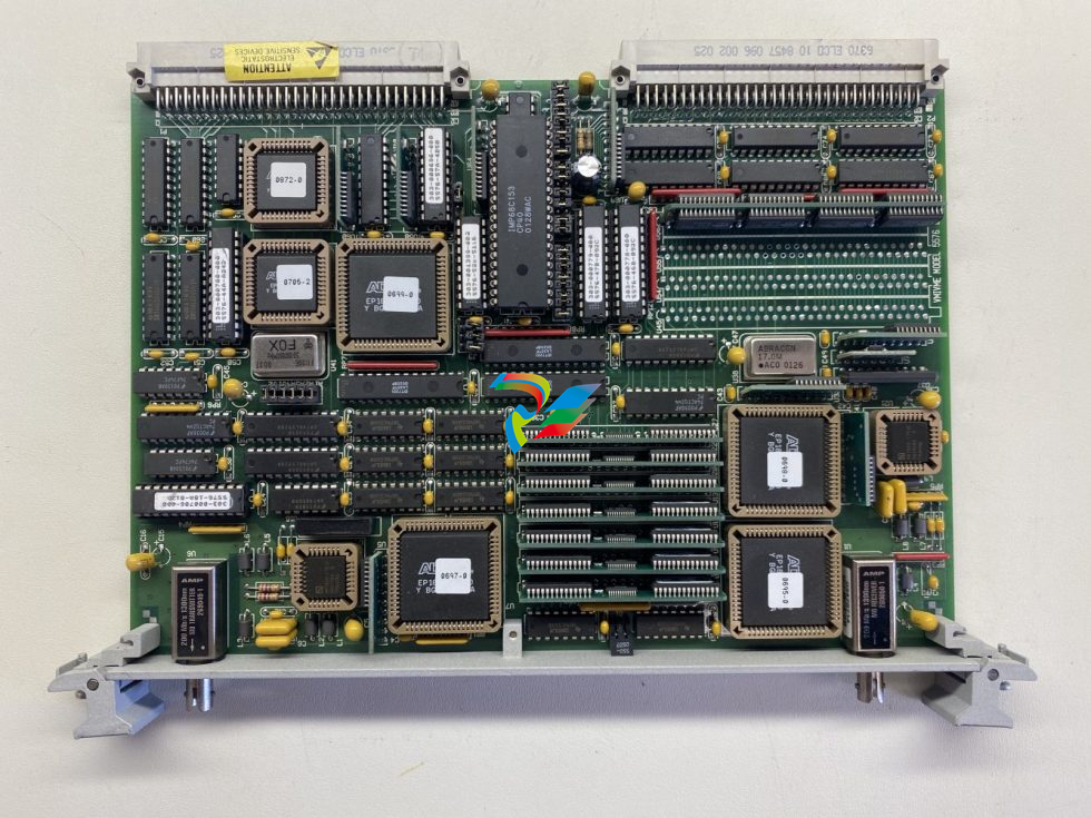
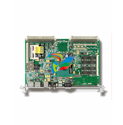
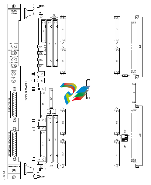 Motorola MVME162 Embedded Controller
 -
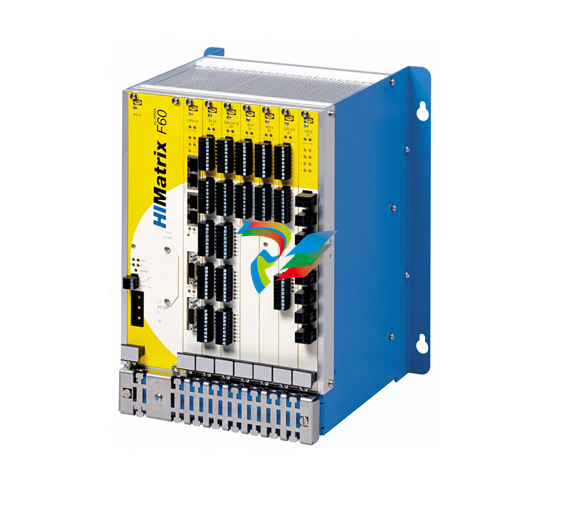 HIMatrix Safety-Related Controller System Manual for the Modular Systems
 -
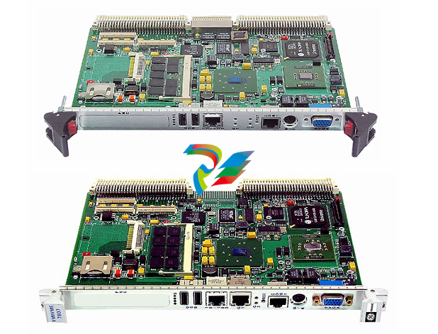
 Motorola MVME2400 Series VME Processor Module
 -
 Sieger System 57
 -
 KONGSBERG MRU product line continuation
 -
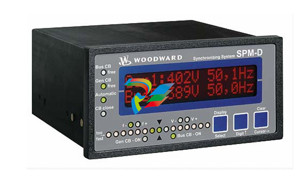
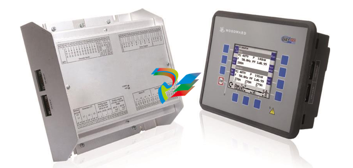 Woodward easYgen-3100/3200 Genset Control for Multiple Unit Operation
 -
 Woodward MFR 300 Multifunction Relay / Measuring
 -
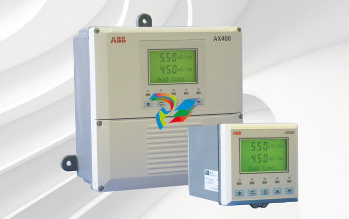 ABB AX410, AX411, AX413, AX416, AX418, AX450, AX455 and AX456 Single and dual input analyzers for low level conductivity
 -
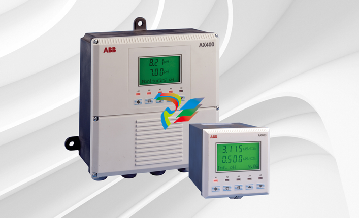 ABB AX410, AX411, AX416, AX450 and AX455 Single and dual input analyzers
 -
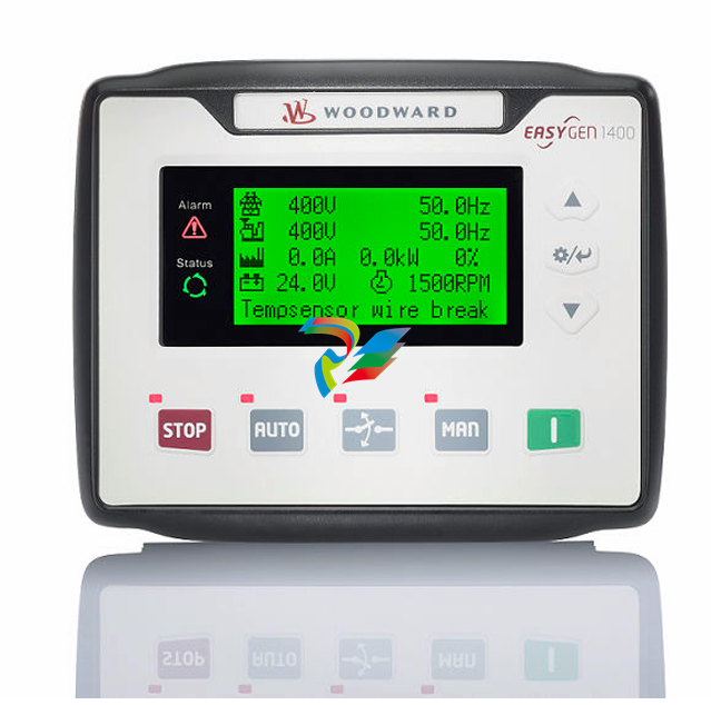 Woodward easYgen-1400 Technical Manual Genset Control
 -
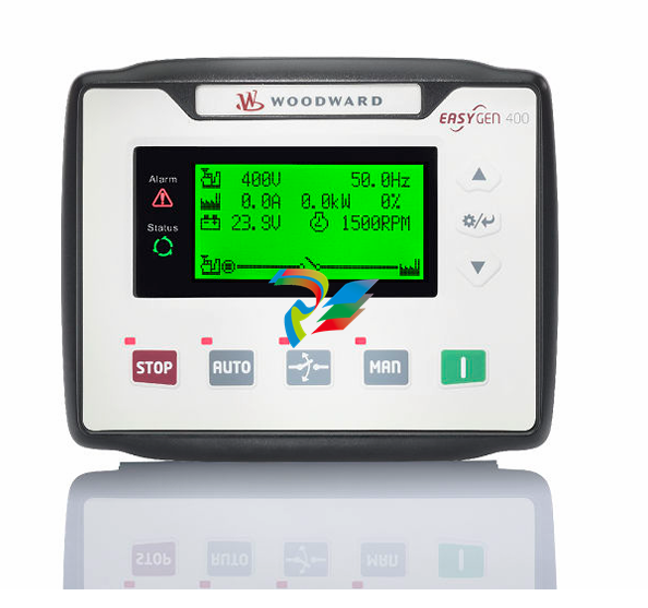 Woodward easYgen-400 Operation Manual Genset Control
 -
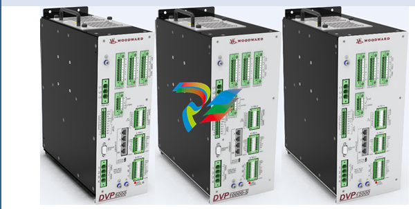 Woodward High Output Digital Valve Positioner (DVP)DVP5000/DVP10000/DVP12000
 -
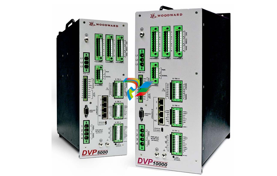 Woodward High Output Digital Valve Positioner DVP5000 and DVP10000
 -
 Woodward TG611-13/-17 Overspeed Test Device Conversion Kit
 -
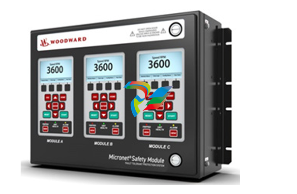 Woodward MicroNet Safety Module (MSM)
 -
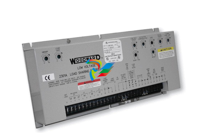 Woodward 2301A Electronic Load Sharing and Speed Control 9905/9907 Series
 -
 Woodward-Service Bulletin 01671
 -
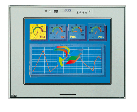
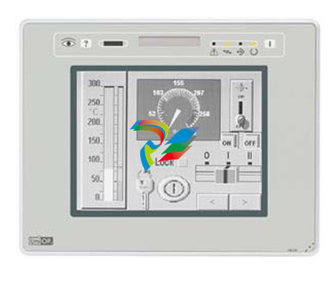
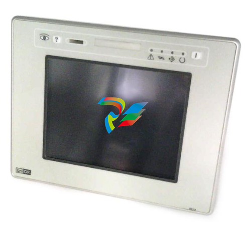
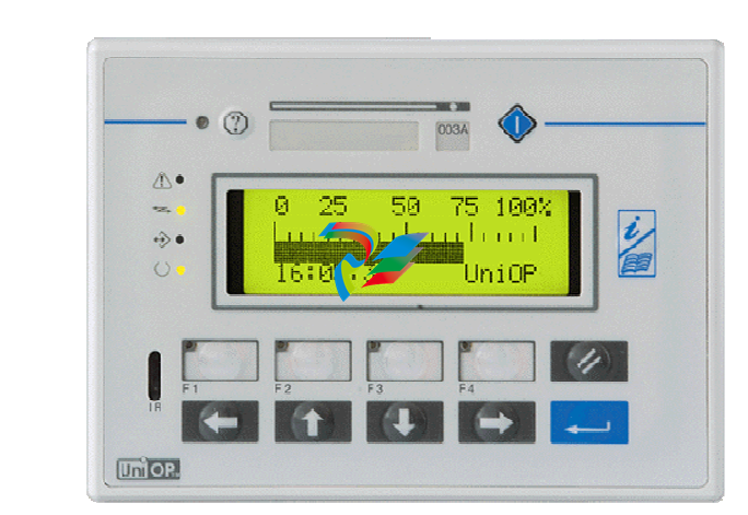
 UniOP eTOP40B 12.1” TFT color display
 -
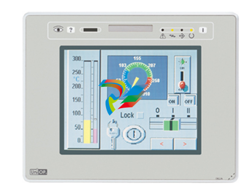
 UniOP eTOP40 TFT Color display
 -
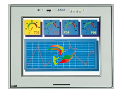
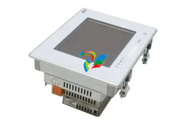
 UniOP eTOP33B 10.4” TFT color display
 -
 UniOP eTOP33C eTOP33-0050 Resistive touchscreen
 -
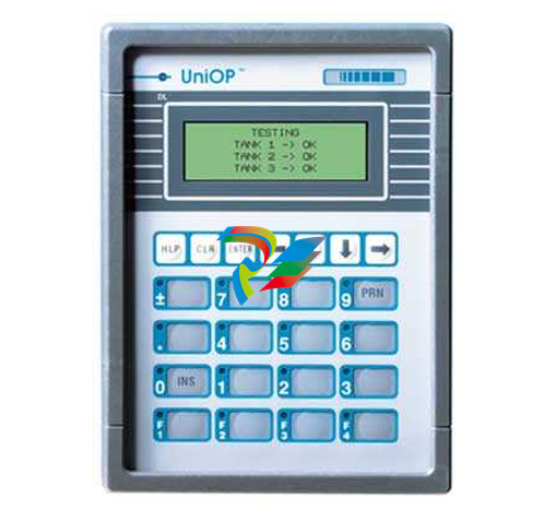
UniOP eTOP30. eTOP32 eTOP32-0050 Human-machine interface equipment
-
 UniOP eTOP20B and eTOP21B eTOP20B-0050
 -
 UniOP eTOP12 eTOP12-0050 Advanced human-machine interface equipment
 -
 UniOP eTOP11 eTOP11-0050 HMI
 -
 UniOP eTOP06C HMI
 -
 UniOP eTOP06 HMI
 -
 UniOP eTOP05EB eTOP05EB-DF45 HMI
 -
 UniOP eTOP05. eTOP05P Human-machine interface equipment
 -
 UniOP eTOP03 eTOP03-0046
 -
 UniOP eTOP507 507U2P1 eTOP Series 500 Human-Machine Interface
 -
 UniOP eTOP307
 -
 UniOP ETT-VGA Human-machine interface touch unit
 -
 UniOP ePAD32B, ePAD33B and ePAD33BT ePAD33B-0350
 -
 UniOP ePAD05 and ePAD06
 -
 UniOP CP02R-04 Human-machine interface
 -
 UniOP ERT-16 - Industrial PLC Workstation
 -
 UniOP ePAD03 and ePAD04
 -
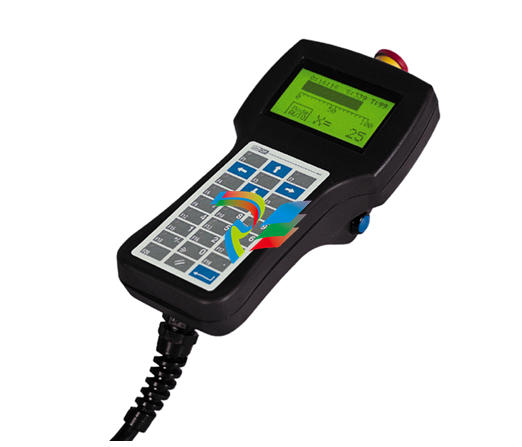 UNIOP EPALM10-DA71 state-of-the-art handheld HMI
 -
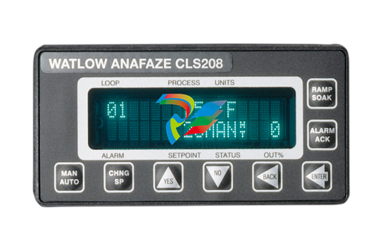 Watlow SERIES CLS200 SPECIFICATION SHEET
 -
 Detailed Explanation of B&R Power Panel 300/400: The Core of Industrial Automation Control
 -
 YOKOGAWA Models ANB10S, ANB10D, ANR10S, ANR10D Node Units (for FIO)
 -
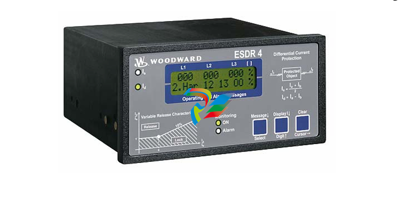 Woodward ESDR 4 Current Differential Protection Relay
 -
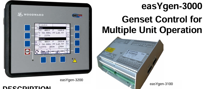 Woodward easYgen-3000 Genset Control for
 -
 Woodward CPC-II Current-to-Pressure Converter
 -
 Woodward 8290-189-EPG-installation-manual 8290-044
 -
 Woodward Product Change Notification 06946A
 -
 Woodward Product Change Notification 06912
 -
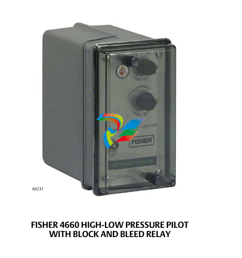 Fisher™ 4660 High-Low Pressure Pilot
 -
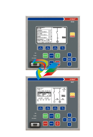 Flexible digital protection and control equipment SYMAP®
 -
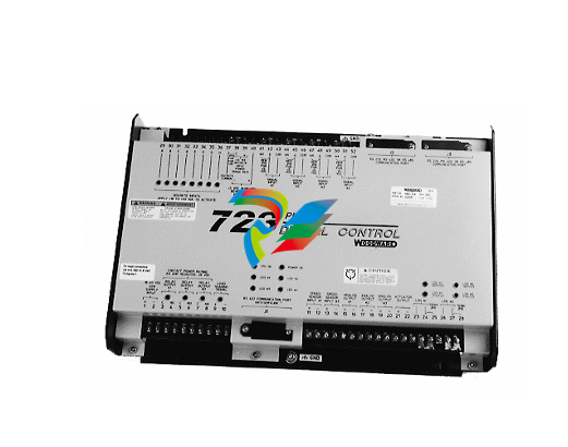 Woodward 723PLUS Digital Control
 -
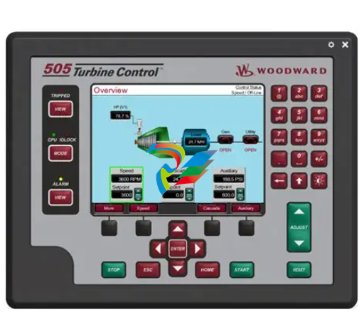 Woodward 505 Digital Controller For steam turbineses
 -
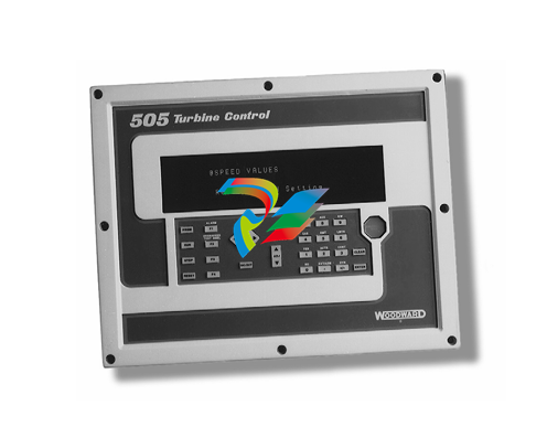 Woodward 85018V2 505E Digital Governor for Extraction Steam Turbines
 -
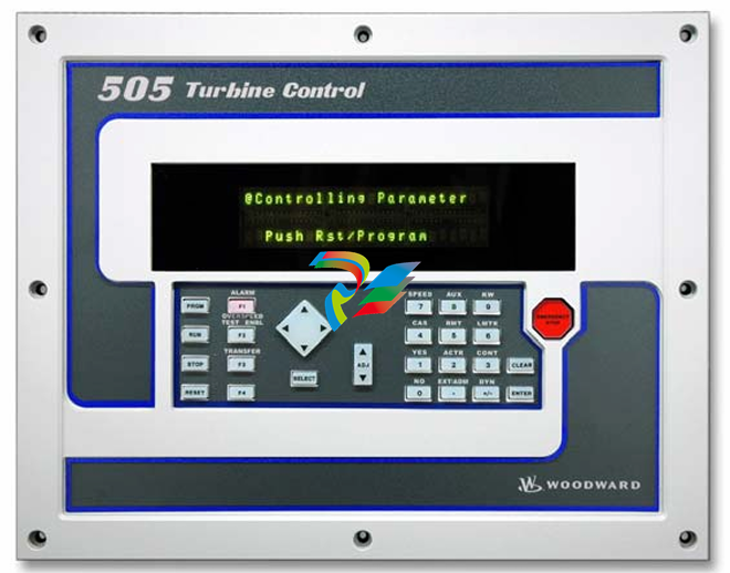
Woodward 85018V1 Turbine Control Parameters
-
Woodward 26871 505 Enhanced Digital Control for Steam Turbines
-
 Woodward 03365 505E (Extraction / Admission)
 -
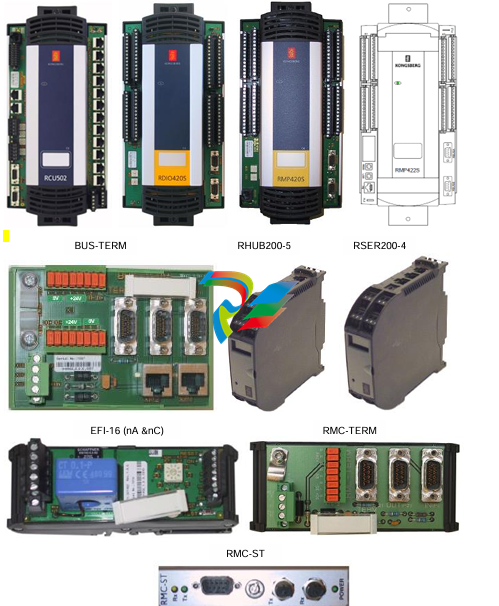
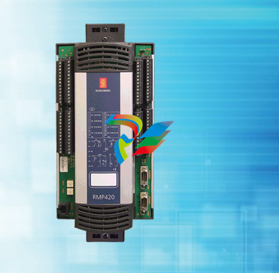 KONGSBERG RMP420-Remote Multipurpose Input/Output
 -
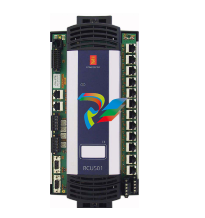 KONGSBERG RCU501 Remote Controller Unit
 -
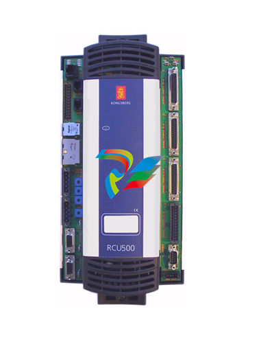 KONGSBERG RCU500 Remote Controller Unit
 -
 K-Gauge TOP KONGSBERG Tank Overfill Protection SystemFeatures
 -
 Kongsberg DPS112 DGNSS (DGPS/DGLONASS) sensor
 -
 Kongsberg d0000930-presafe-atex-report signed
 -
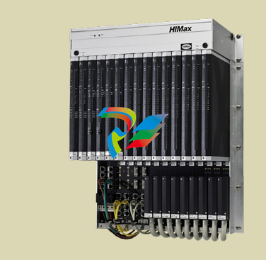 HIMax TECHNICAL FACTS X Series
 -
 GE Multilin F650
 -
 GE MIF II - Legacy
 -
 GE PQM II Power QualIty Meter
 -
 Hydran 201Ti Mark IV Essential DGA monitoring for transformers
 -
 alstom AMS42/84 5B Amplifier SystemAmplifier Technology at its Best.
 -
 GE VMIVME-5576 Fiber-Optic Reflective Memory with Interrupts
 -
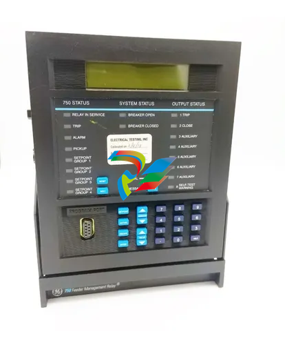 GE Multilin 750/760 - Legacy Feeder Protection System
 -
 GE Fanuc Automation VMICPCI-7806 Specifications
 -
 VMIVME-7807 VME-7807RC* Intel® Pentium® M-Based VME SBC
 -
 GE Fanuc Automation VMIVME-7750 Specifications
 -
 FOXBORO Compact FBM240. Redundant with Readback, Discrete
 -
 FOXBORO FBM208/b, Redundant with Readback, 0 to 20 mA I/O Module
 -
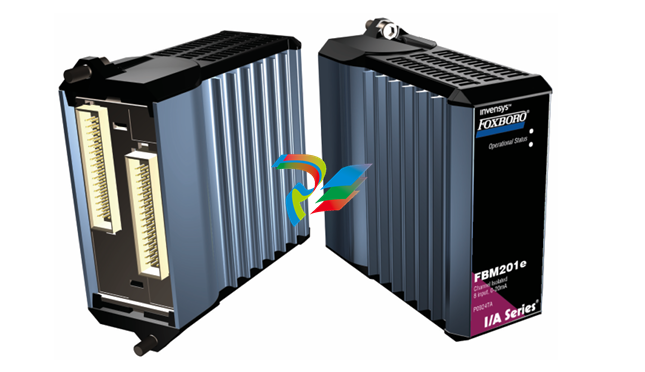 FOXBORO FBM201e Analog Input (0 to 20 mA) Interface Modules
 -
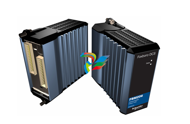 Foxboro DCS FBM206 Pulse Input Module
 -
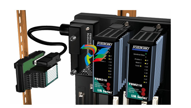 FOXBORO FBM216 HART® Communication Redundant Input Interface Module
 -
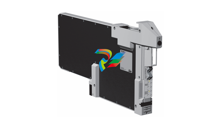 FOXBORO Z-Module Control Processor 270 (ZCP270)
 -
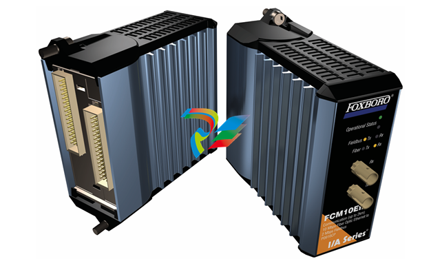 FOXBORO Fieldbus Communications Module, FCM10Ef
 -
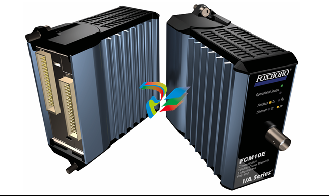 FOXBORO Fieldbus Communications Module, FCM10E
 -
 Foxboro DCS Compact FBM241/c/d, Redundant, Discrete I/O Modules
 -
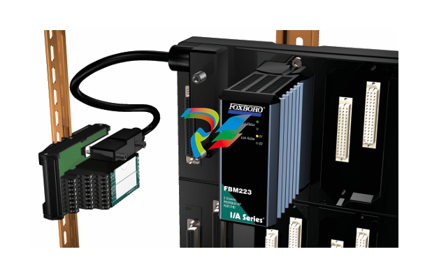
Foxboro FBM223 PROFIBUS-DP™ Communication Interface Module
-
 Foxboro DCS FBM204. 0 to 20 mAI/OModule
 -
Foxboro FBM239, Discrete 16DI/16DO Module
-
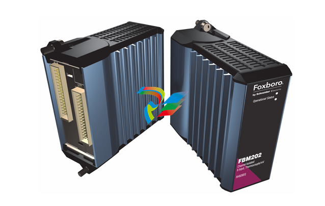
Foxboro FBM202 Thermocouple/mV Input Module
-
 Foxboro E69F Current-to-Pneumatic Signal Converter
 -
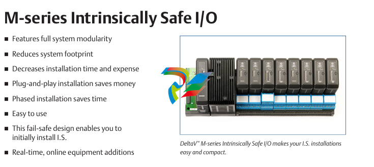 EMERSON M-series Intrinsically Safe I/O
 -
 MVME6100 Series VMEbus Single-Board Computer
 -
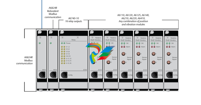 Configuration for AMS 6500 Protection Monitors
 -
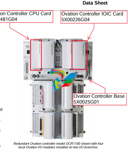 Ovation™ Controller Model OCR1100 (5X00481G04/5X00226G04)
 -
 ABB UCU-22, UCU-23 andUCU-24control units