OMRON C500-CT012 PLC
OMRON C500-CT012 PLC
9-16 Extended Data Memory (EM) Area
The EM Area is supported by the CJ1 and CJ1-H CPU Units only. It is divided
into 7 banks (0 to C) that each contain 32.768 words. EM Area addresses
range from E0_00000 to EC_32767. This data area is used for general data
storage and manipulation and is accessible only by word.
Data in the EM Area is retained when the PLC’s power is cycled or the PLC’s
operating mode is changed from PROGRAM mode to RUN/MONITOR mode
or vice-versa.
Although bits in the EM Area cannot be accessed directly, the status of these
bits can be accessed with the BIT TEST instructions, TST(350) and
TSTN(351).
Bits in the EM Area cannot be force-set or force-reset.
Specifying EM Addresses
1.2.3...
There are two ways to specify an EM address: the bank and address can be
specified at the same time or an address in the current bank can be specified
(after changing the current bank, if necessary). In general, we recommend
specifying the bank and address simultaneously.
1. Bank and Address Specification
With this method, the bank number is specified just before the EM address.
For example, E2_00010 specifies EM address 00010 in bank 2.
2. Current Bank Address Specification
With this method, just the EM address is specified. For example, E00010
specifies EM address 00010 in the current bank. (The current bank must
be changed with EMBC(281) to access data in another bank. A301 con
tains the current EM bank number.)
The current bank will be reset to 0 when the operating mode is changed
from PROGRAM mode to RUN/MONITOR mode, unless the IOM Hold Bit
(A50012) is ON. The current bank is not changed as the program proceeds
through cyclic tasks and the current bank will be returned to its original val
ue (in the source cyclic task) if it has been changed in an interrupt task
Words in the EM Area can be indirectly addressed in two ways: binary-mode
and BCD-mode.
Binary-mode Addressing (@E)
When a “@” character is input before a EM address, the content of that EM
word is treated as binary and the instruction will operate on the EM word in
the same bank at that binary address. All of the words in the same EM bank
(E00000 to E32767) can be indirectly addressed with hexadecimal values
0000 to 7FFF and words in the next EM bank (E00000 to E32767) can be
addressed with hexadecimal values 8000 to FFFF.
@E1_00100
@E00100
0200
0200
E1_00512
Address actually used.
E0_00512
Address actually used.
BCD-mode Addressing (
*
(When the current
bank is bank 0.)
E)
When a “*” character is input before a EM address, the content of that EM
word is treated as BCD and the instruction will operate on the EM word in the
same bank at that BCD address. Only part of the EM bank (E00000 to
E09999) can be indirectly addressed with BCD values 0000 to 9999.
*E1_00100
*E00100
0200
0200

E1_00200
Address actually used.
▲
E0_00200
Address actually used.
(When the current
bank is bank 0.)
Part of the EM Area can be converted for use as file memory with settings in
the PLC Setup. All EM banks from the specified bank (EM File Memory Start
ing Bank) to the last EM bank will be converted to file memory.
Once EM banks have been converted to file memory, they cannot be
accessed (read or written) by instructions. An Illegal Access Error will occur if
a file-memory bank is specified as an operand in an instruction.
The following example shows EM file memory when the EM File Memory
Starting Bank has been set to 3 in the PLC Setup.
Example:
EM File Memory Starting Bank
EM bank number
set to 3 in the PLC Setup
EM file memory
(Cannot be accessed
from instructions.)
9-17 Index Registers
The sixteen Index Registers (IR0 to IR15) are used for indirect addressing.
Each Index Register can hold a single PLC memory address, which is the
absolute memory address of a word in I/O memory. Use MOVR(560) to con
vert a regular data area address to its equivalent PLC memory address and
write that value to the specified Index Register. (Use MOVRW(561) to set the
PLC memory address of a timer/counter PV in an Index Register.)
Note Refer to Appendix D Memory Map of PLC Memory Addresses for more details
on PLC memory addresses
| User name | Member Level | Quantity | Specification | Purchase Date |
|---|



-
 SELSEL-T401L Ultra-High-Speed Line Relay
 -
 SEL SEL-T400L Time-Domain Line Protection
 -
 SEL SEL-2664S Stator Ground Protection Relay
 -
 SEL SEL-787-2/-3/-4 Transformer Protection Relay
 -
 SEL SEL-787 Transformer Protection Relay
 -
 SEL SEL-751 Feeder Protection Relay
 -
 SEL SEL-700G Generator Protection Relay
 -
 SEL-487E Transformer Protection Relay
 -
 SEL-400G Advanced Generator Protection System
 -
 SEL SEL-387E Current Differential and Voltage Relay
 -
 SEL SEL-387A Current Differential and Overcurrent Relay
 -
 SEL SEL-387 Current Differential and Overcurrent Relay
 -
 SEL SEL-300G Generator Relay
 -
 SEL SEL-700BT Motor Bus Transfer Relay
 -
 CTI 2500 Series® Slice Ethernet Remote I/O System
 -
 CTI 2500 Series® Compact Programmable Automation Control System
 -
 CTI 2500 Series® Classic Programmable Automation Control System
 -
 CTI 2500 Series® Bases
 -
 SHINKAWA VM-25 Condition Monitoring System UPDATED
 -
 SHINKAWA VM-5 SERIES OPTIONS
 -
 ABB SACO 64D4 Annunciator unit
 -
 ABB SPAU 140 C Synchro-check relay
 -
 EATON Instructions for the FP-5000
 -
 HONEYWELL TDC 3000X Advanced Process Manager
 -
 HONEYWELL ENHANCED MICRO TDC 3000
 -
 VIBRO-METER VM600Mk2/ VM600 RPS6U rack power supplies
 -
 VIBRO-METER VM600Mk2/ VM600 ABE056 slimline rack
 -
 VIBRO-METER VM600Mk2 RLC16Mk2 relay modules
 -
 VIBRO-METER VM600Mk2 MPC4Mk2 + IOC4Mk2 machinery protection and condition monitoring modules
 -
 VIBRO-METER VM600Mk2 CPUMMk2 + IOCNMk2 rack controller and communications interface module
 -
 VIBRO-METER VM600Mk2 CPUMMk2 + IOCNMk2 rack controller and communications interface module
 -
 ADLINK PCI/PCIe-7300A, cPCI-7300 32-CH 80 MB/s High-Speed Digital I/O Cards
 -
 ADLINK cPCI-7248/7249R 48-CH DIO & Timer/Counter Cards
 -
 ADLINK PCI-7230/7233/7234. LPCI/LPCIe/cPCI-7230 32-CH Isolated DIO Cards
 -
 ADLINK cPCI-6965 Series Value 6U CompactPCI® Intel® Core™2 Duo
 -
 ADLINK cPCI-6910 Series 6U CompactPCI® Dual-Core Intel® Xeon® Processor LV / ULV Universal Blade
 -
 ADLINK CPCI-6670 6U CompactPCI Low Power Pentium® III SBC
 -
 ADLINK cPCI-6625/6 Series 6U CompactPCI® PlusIO blade with Intel® Core™ i7/i3 Processor
 -
 ADLINK 3U CompactPCI CPU Modules
 -
 ADLINK CM-435 Extreme Rugged™ PC/104 Single Board Computer
 -
 ADLINK PCI-8254/8258 DSP-based 4/8-axis Advanced Motion Controllers
 -
 ADLINK NuPRO-E43 PICMG® 1.3 Full-Size LGA1151 with 6th/7th Generation Intel® Core™ i7/i5/i3
 -
 ADLINK DLAP-211-JNX/DLAP-211-JT2/ DLAP-211-Nano
 -
 Hirschmann RS30-1602O6O6SDAE compact OpenRail managed Ethernet switches
 -
Hirschmann RS30-0802O6O6SDAE Ethernet switch
-
 Hirschmann RS20-1600T1T1SDAE Management-type Ethernet switch
 -
 Hirschmann OCTOPUS 24M Limited Availability/Passive
 -
 Hirschmann MSP30-24040SCZ9MRHHE3A
 -
 Hirschmann MAR1040-4C4C4C4C9999SMMHRHHXX.X. Gigabit Ethernet Switch configurator
 -
 Hirschmann Industrial Ethernet Rail Switch SPIDER II, SPIDER II Giga, SPIDER II PoE
 -
 Hirschmann Industrial Ethernet Firewall EAGLE One
 -
 Hirschmann Industrial Security Router EAGLE20/30
 -
 Hirschmann Description and operating instructions RS2-xTX/xFX EEC
 -
 Basler Electric DECS-200 Digital Excitation Control System
 -
 Basler Electric GENERATOR PROTECTION SYSTEM BE1-GPS100
 -
 Jaquet FT3000 Speed measurement system
 -
 Hirschmann Industrial Ethernet Ruggedized Switch MACH1000 Family
 -
 Basler Electric BESTCOMSPlus®
 -
 ETEL AccurET MODULAR 300 EA-P2M-300-xxxxxA controller
 -
 Basler Electric ES Series Protection Relays
 -
 ABB Multifunction Protection and Switchbay Control Unit REF542plus
 -
 EMERSON AMS 2140 Machinery Health Analyzer
 -
 Hirschmann Industrial Ethernet Rail Switch RS20 Basic Family
 -
 GE Grid Solutions P40U Px40 USB Adaptor
 -
 ABB ontinuous Gas Analyzers AO2000 Series AO2040CU Ex Central Unit in Category 2G
 -
 ABB Advance Optima AO2000 Series Continuous gas analyzers Models AO2020. AO2040
 -
 Advance Optima Module Uras 14
 -
 SAACKE control optimization
 -
 SAACKE se@vis efficiency monitor
 -
 SAACKE se@vis pro
 -
 SAACKE se@vis eco
 -
 SAACKE se@vis compact
 -
 HIRSCHMANN Industrial ETHERNET Switch MICE MS20/MS30
 -
 HIRSCHMANN MICE Media modules
 -
 Kongsberg GL-10 Level Switch
 -
 B&R ACOPOSinverter P74 frequency converter
 -
 Beckhoff CX2020 | Basic CPU module (service phase)
 -
 Beckhoff CX1010 | Basic CPU module (service phase)
 -
 Beckhoff CX5120 | Embedded PC with Intel Atom® E3815
 -
 Beckhoff CP69xx-xxxx-0010 | Economy built-in Control Panel with DVI/USB Extended interface
 -
 Beckhoff CP29xx-0000 | Multi-touch built-in Control Panel with DVI/USB Extended interface
 -
 SAACKE Monoblock Rotary Cup Burner SKVJ-M
 -
 ABB Plantguard Fault Tolerant Technology Architecture and Software
 -
 OMRON H8PR-8/H8PR-8P H8PR-16/H8PR-16P H8PR-24/H8PR-24P Rotary Positioner
 -
 ABB PFSA107-Z42 DTU Stressometer Digital Transmission Unit
 -
 Nidec Mentor MP
 -
 IBA ibaNet-E
 -
 IBA FO Connection to Reflective Memory
 -
 IBA FO Connection to Siemens Systems
 -
 IBA Interface Cards For Fiber Optic Connections
 -
 IBA Field and Drive Buses
 -
 IBA ibaPADU-S Modular System
 -
 IBA ibaMAQS
 -
 STUCKE SYMAP®ARC
 -
 STUCKE SYMAP®R
 -
 STUCKE SYMAP®Compact
 -
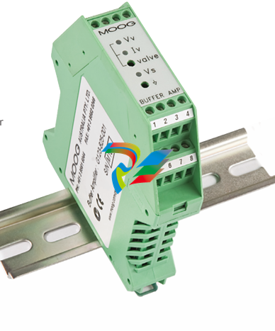 MOOG G123-825-001 BUFFER AMPLIFIER
 -
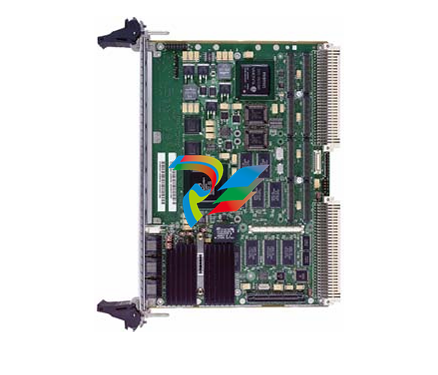 Motorola MVME5100 Series VME Processor Modules
 -
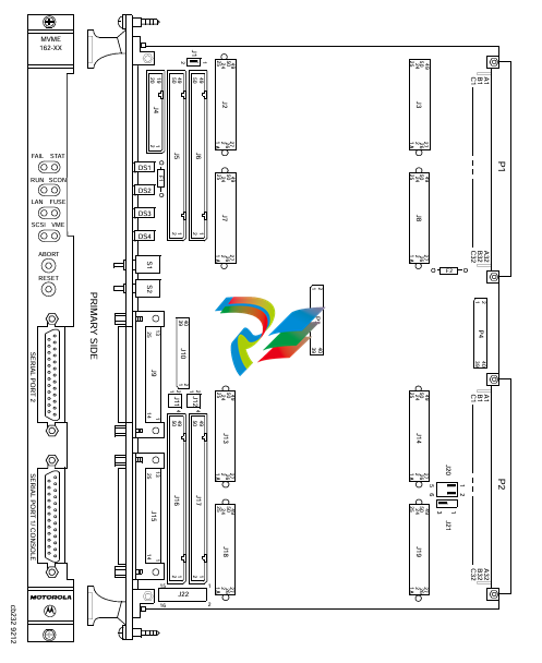 Motorola MVME162 Embedded Controller
 -
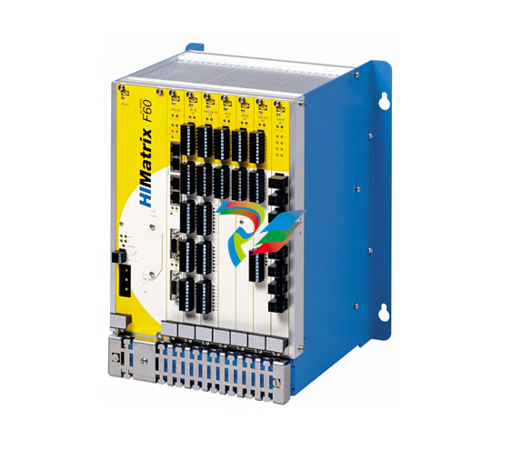 HIMatrix Safety-Related Controller System Manual for the Modular Systems
 -
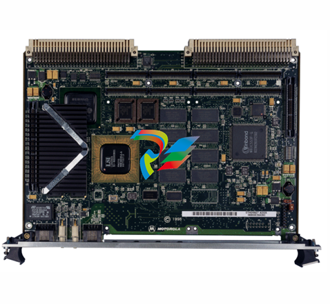 Motorola MVME2400 Series VME Processor Module
 -
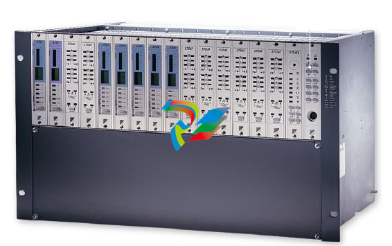 Sieger System 57
 -
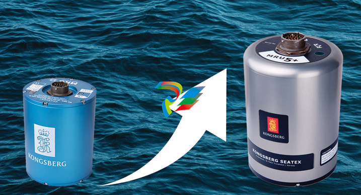 KONGSBERG MRU product line continuation
 -
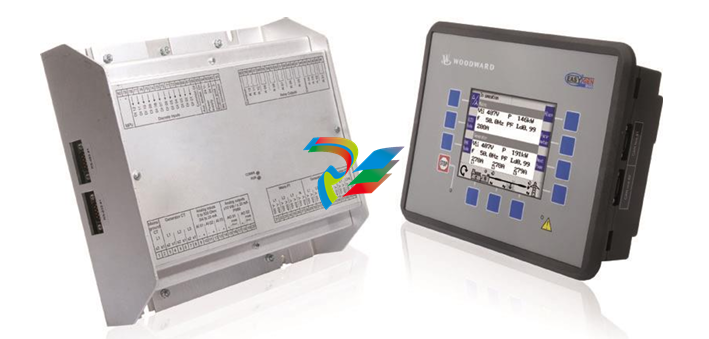 Woodward easYgen-3100/3200 Genset Control for Multiple Unit Operation
 -
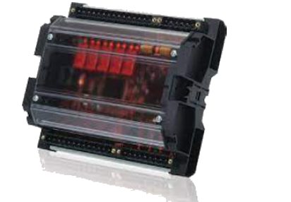 Woodward MFR 300 Multifunction Relay / Measuring
 -
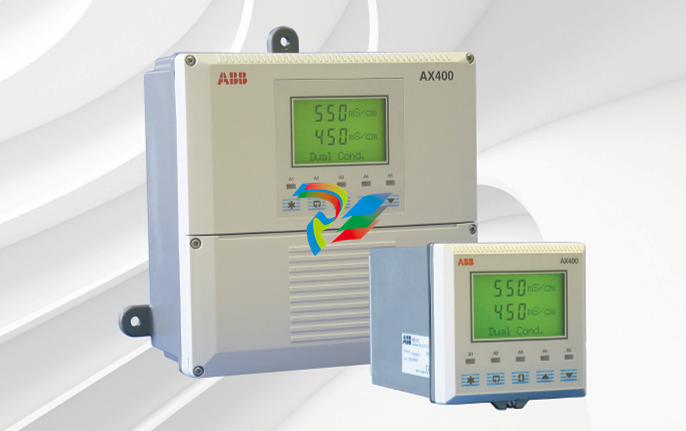 ABB AX410, AX411, AX413, AX416, AX418, AX450, AX455 and AX456 Single and dual input analyzers for low level conductivity
 -
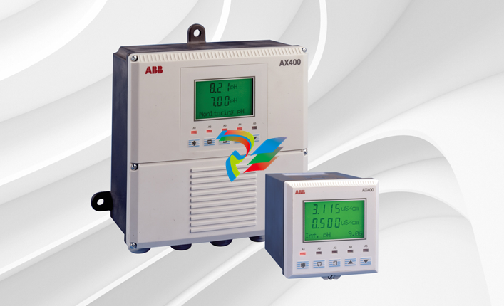 ABB AX410, AX411, AX416, AX450 and AX455 Single and dual input analyzers
 -
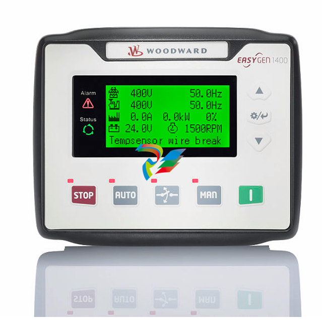 Woodward easYgen-1400 Technical Manual Genset Control
 -
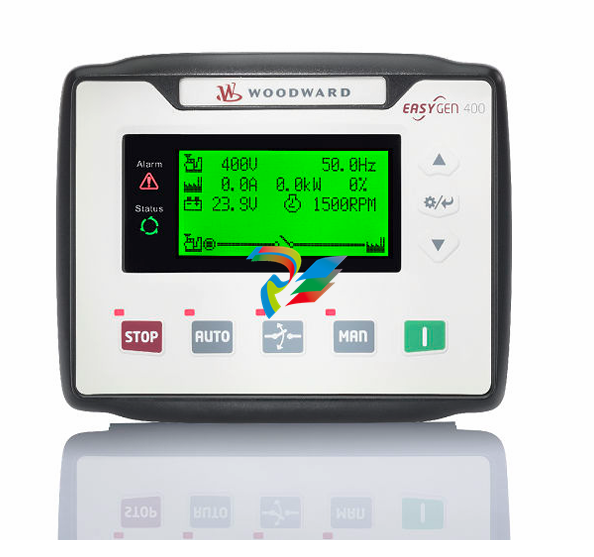 Woodward easYgen-400 Operation Manual Genset Control
 -
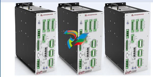 Woodward High Output Digital Valve Positioner (DVP)DVP5000/DVP10000/DVP12000
 -
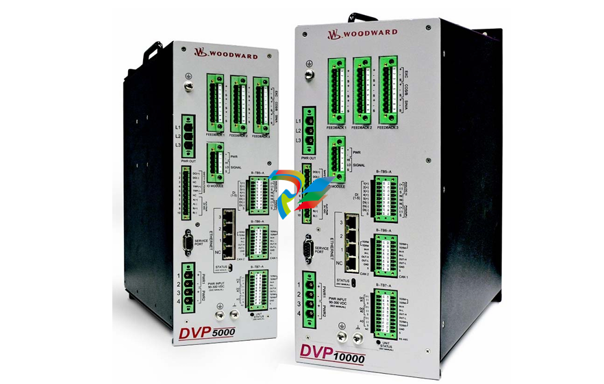 Woodward High Output Digital Valve Positioner DVP5000 and DVP10000
 -
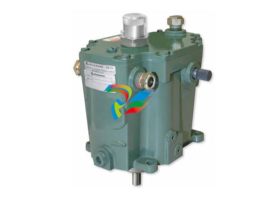 Woodward TG611-13/-17 Overspeed Test Device Conversion Kit
 -
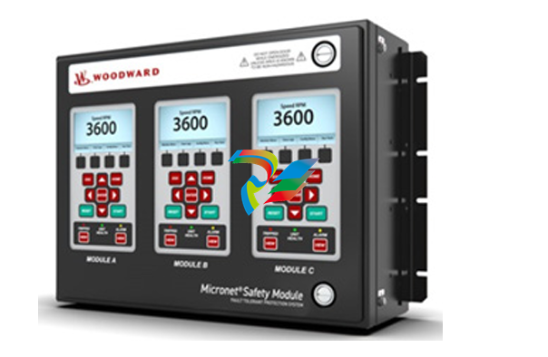 Woodward MicroNet Safety Module (MSM)
 -
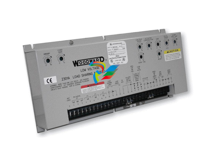 Woodward 2301A Electronic Load Sharing and Speed Control 9905/9907 Series
 -
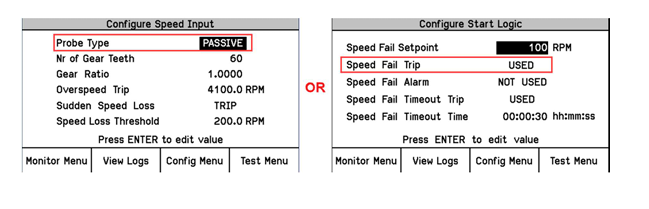 Woodward-Service Bulletin 01671
 -
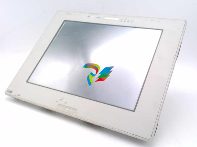 UniOP eTOP40B 12.1” TFT color display
 -
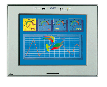 UniOP eTOP40 TFT Color display
 -
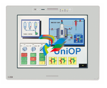 UniOP eTOP33B 10.4” TFT color display
 -
 UniOP eTOP33C eTOP33-0050 Resistive touchscreen
 -
UniOP eTOP30. eTOP32 eTOP32-0050 Human-machine interface equipment
-
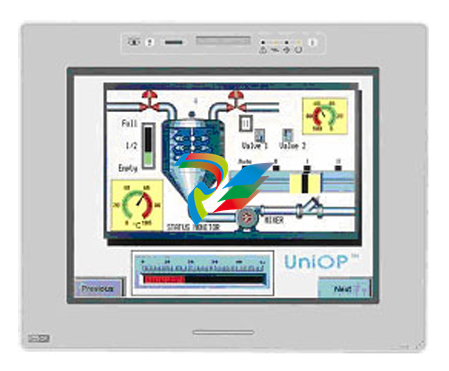 UniOP eTOP20B and eTOP21B eTOP20B-0050
 -
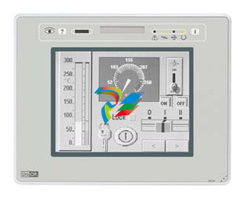 UniOP eTOP12 eTOP12-0050 Advanced human-machine interface equipment
 -
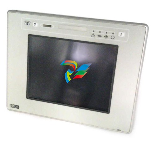 UniOP eTOP11 eTOP11-0050 HMI
 -
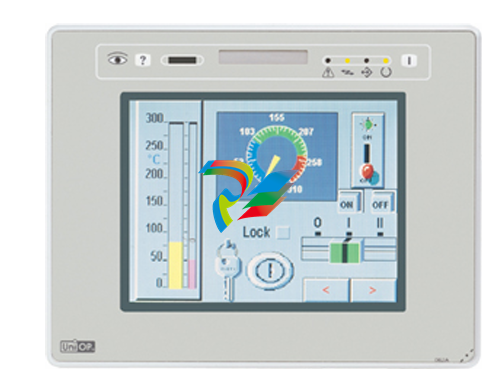 UniOP eTOP06C HMI
 -
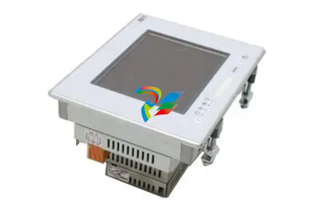 UniOP eTOP06 HMI
 -
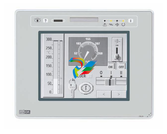 UniOP eTOP05EB eTOP05EB-DF45 HMI
 -
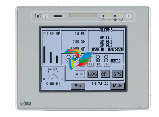 UniOP eTOP05. eTOP05P Human-machine interface equipment
 -
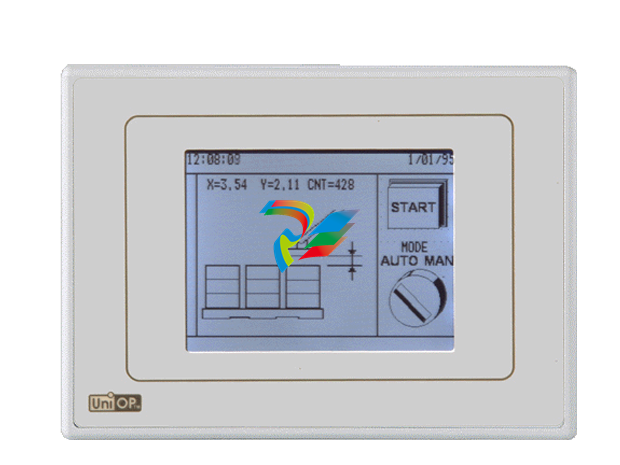 UniOP eTOP03 eTOP03-0046