MotorolaMVME55006E Single-Board Computer Installation and Use
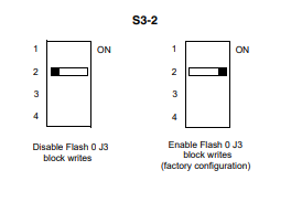
This switch supports the Intel J3 Flash family write protect feature. Set to OFF, it enables the
lock-down mechanism. Blocks locked down cannot be unlocked with the unlock command. The
switch must be set to ON in order to override the lock-down function and enable blocks to be
erased or programmed through software. Refer to the Intel J3 Flash data sheet, listed in
Appendix C, Related Documentation, for further details.
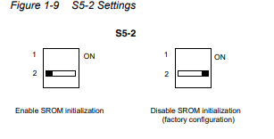
SROM Initialization Enable Switch (S5-2)
This switch enables/disables the GT-64260B SROM initialization. When set to 2, it enables the
GT-64260B device initialization via I2C SROM. Set to ON disables this initialization sequence.
SROM Initialization Enable Switch (S5-2)
This switch enables/disables the GT-64260B SROM initialization. When set to 2, it enables the
GT-64260B device initialization via I2C SROM. Set to ON disables this initialization sequence.
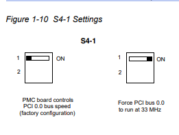
PCI Bus 0.0 Speed Switch (S4-1)
This switch can force PCI bus 0.0 to run at 33 MHz rather than the standard method of allowing
the PMC board to control whether the bus runs at 33 MHz or 66 MHz. Set to 1, it allows the
PMC board to choose the PCI 0.0 bus speed. Set to ON forces PCI bus 0.0 to run at 33 MHz.
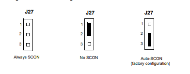
9 VME SCON Select Header (J27)
A 3-pin planar header allows the choice for auto/enable/disable SCON VME configuration. A
jumper installed across pins 1-2 configures for SCON disabled. A jumper installed across pins
2-3 configures for auto SCON. No jumper installed configures for SCON always enabled.
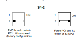
0 PCI Bus 1.0 Speed Switch (S4-2)
This switch can force PCI bus 1.0 to run at 33 MHz rather than the standard method of allowing
the PMC board to control whether the bus runs at 33 MHz or 66 MHz. Set to 1, it allows the
PMC board to choose the PCI 1.0 bus speed. Set to ON forces PCI bus 1.0 to run at 33 MHz.
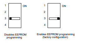
1 EEPROM Write Protect Switch (S3-3)
This switch enables/disables programming of the on-board EEPROMs as a means of protecting
the contents from being corrupted. Set to 1, it disables EEPROM programming by driving the
WP pin to a logic high. Set to ON to program any of the EEPROMs at addresses A0, A6, A8,
and/or AA.
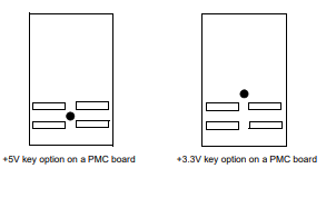
Setting the PMC Vio Keying Pin
Signalling voltage (Vio) is determined by the location of the PMC Vio keying pin. Each site can
be independently configured for either +5V or +3.3V signalling. The option selected can be
determined by observing the location of the Vio keying pin.
Installing the RAM5500 Module
Procedure
To upgrade or install a RAM5500 module, refer to and proceed as follows:
1. Attach an ESD strap to your wrist. Attach the other end of the ESD strap to the
chassis as a ground. The ESD strap must be secured to your wrist and to ground
throughout the procedure.
2. Perform an operating system shutdown. Turn the AC or DC power off and remove
the AC cord or DC power lines from the system. Remove the chassis or system
cover(s) as necessary for access to the VME boards.
3. Carefully remove the MVME5500 from its VME card slot and lay it flat, with
connectors P1 and P2 facing you.
4. Inspect the RAM5500 module that is being installed on the MVME5500 host board
to ensure that standoffs are installed in the four mounting holes on the module.
5. With standoffs installed in the four mounting holes on the RAM5500 module, align
the standoffs and the P1 connector on the module with the four holes and the P4
connector on the MVME5500 host board and press the two connectors together
until they are firmly seated in place.
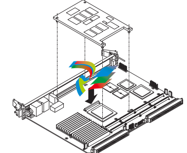
6. Turn the entire assembly over and fasten the four short Phillips screws to the
standoffs of the RAM5500.
-
 Hirschmann RS20-1600M2T1SDAEHH03.1.02 Rail Switch
 -
 Hirschmann BRS30-24TX Industrial Rail Switch
 -
 Hirschmann RSPM20-4T14T1EV9HHS999.9.99 Managed Ethernet Switch
 -
 Hirschmann BELDEN RS40-0009CCCCSDAPHH09.0.14 / RS400009CCCCSDAPHH09014
 -
Hirschmann RS40 Rail Switch RS40-0009CCCCSDAE
-
 Hirschmann BELDEN RS30-0802T1T1SDAP / RS300802T1T1SDAP Fully Managed Layer 2 Compact Rail Switch
 -
 Hirschmann BELDEN RS20-0800M2M2SDAUHH / RS200800M2M2SDAUHH
 -
 Hirschmann EAGLE30-04022O6TT999SCCY9HSE3F Industrial Firewall Router Switch
 -
 Hirschmann RS20-1600T1T1SDAEHH09.0.14 RS20 Rail Mount Ethernet Switch
 -
 Hirschmann EAGLE0200T1T1TDDY90000HHE05.3.03 Industrial Security Router
 -
Hirschmann - BELDEN MIPP-AD-1L9P
-
 HIRSCHMANN RSPM20-4Z64Z6TV9HHS9 942 106-999 RAIL SAFETY SWITCH
 -
 HIRSCHMANN FIBEROPTIC MODULE FIP P/N: OZDFIPG3T
 -
 HIRSCHMANN RS20-1600M2M2SDAUHH Ethernet rack-mounted switch
 -
 HIRSCHMANN BELDEN RS20-0400T1T1SDAEHH04.0.01 / RS200400T1T1SDAEHH04001
 -
HIRSCHMANN MM2-4FXM3 MICE Media Module
-
HIRSCHMANN RS20-0800M2M2SDAE Industrial Ethernet Rail Switch
-
 Hirschmann RS20-2400T1T1SDAP / RS20-2400T1T1SDAPHH05.0.02
 -
 GE MLJ1005B010H00C MLJ Digital Synchromism Check
 -
 ALSTOM MICROTECH DX21-M2 Digital Excitation Controller
 -
HIRSCHMANN BRS20-1200ZZZZ-STCY99HHSES
-
 HIRSCHMANN MM3-4FXM2 MICE Media Module
 -
Hirschmann RSB20-0800T1T1SAABHH 8Port ENet Rail Switch RSB20
-
 Hirschmann MACH102-8TP Ethernet Switch
 -
 SAACKE DDZ-M marine steam pressure atomizer
 -
 SAACKE SKV-A marine rotary cup atomizer
 -
 SAACKE Seavis HMI05e
 -
 Kollmorgen MMC-SD-2.0-230 Servo Drive 100-240VAC 2KW 10A Output 3PH 100-240VAC
 -
 Kollmorgen Servo drive CR10550
 -
 Kollmorgen AKD-P01207-NACN-0054 Servo Driver
 -
 Kollmorgen S406M-CA-036 Servostar
 -
.png) Kollmorgen AKD-B02407-NAAN-0000 Digital Servo Drive
Kollmorgen AKD-B02407-NAAN-0000 Digital Servo Drive -
 Kollmorgen SERVOSTAR S406AM-CA Digital Servo Drive
 -
 KOLLMORGEN SERVOSTAR 603-AS SERVO AMPLIFIER_SERVOSTAR603AS_S60301
 -
Kollmorgen S700 Servo Controller (S70602-NANANA-NA)
-
 Kollmorgen MPK411 controller
 -
 KOLLMORGEN MMC-SD-1.3-460-D Smart Drive
 -
 KOLLMORGEN AKM21C-CKB2AA-00 / AKM21CCKB2AA00 Servomotor
 -
 BECKHOFF AX5106-0000-0200 | Digital Compact Servo Drives 1-channel
 -
 BECKHOFF C3620-0000 INDUSTRIAL COMPUTER (MOTORSHELVES)
 -
 Beckhoff EK1960-0000 TwinSAFE Compact Controller
 -
 Beckhoff C6930-0050 Control Cabinet Industrial PC
 -
 Beckhoff CP7711-0001-0030 Industrial Computer Detection
 -
 Beckhoff CX1001-0111 Embedded PC CPU Module
 -
 Beckhoff C6017-0020 | Ultra-compact Industrial PC
 -
 Beckhoff EK1322 | 2-port EtherCAT P junction with feed-in
 -
 Beckhoff CP2219-0010 Panel
 -
 BECKHOFF C6015-0020 ULTRA COMPACT INDUSTRIAL PC
 -
 BECKHOFF CX2030-0120/Standard CPU Module Embedded PC Windows PLC controller
 -
 Beckhoff CP7721-1090-0020 Panel PC
 -
 Beckhoff PC CPU Module CX5130-0175
 -
 Beckhoff C6920-0050 Control Cabinet
 -
 Beckhoff EL6631 EtherCAT 2-Port Communication Interface, Profinet RT Controller
 -
 Beckhoff CP6202-0001-0060 touch screen panel PC
 -
 Beckhoff CP3916-1002-0000 Multi-Touch Control Panel
 -
 Beckhoff EP1809-0021 | EtherCAT Box, 16-channel digital input, 24 V DC, 3 ms, M8Preferred type
 -
 Beckhoff CX8190 PLC Embedded Industrial PC Ethernet Controller
 -
 Beckhoff CX2100-0914 Power Supply for External
 -
 Beckhoff Automation CP6906-0001-0000 HMI
 -
 Beckhoff EP7342-0002 Module
 -
 Beckhoff CX1020-0112 / CX1100-0910 / CX1020-N010 / CX1100-0003 Windows CPU
 -
 Beckhoff EP7211-0034 EtherCAT Box 1 Channel Motion Interface
 -
 Beckhoff C6240-0030 Control cabinet Industrial PC
 -
 beckhoff motherboard CB1052-0004 CB1052-0004
 -
 Beckhoff AX2006-AS Servo Drive / Variable Frequency Drive
 -
BECKHOFF CP6207-0001-0020 NSMP
-
 Beckhoff C6930-1142-0060 Industrial Computer
 -
 Beckhoff FC7501-0000 interface card
 -
 Beckhoff CX5140-0175 Embedded PC PLC CPU CX5140 Industrial Controller
 -
 Beckhoff CP7802-1100-0010: High-End IP65 Control Panel with DVI/USB Extended Interface
 -
BECKHOFF CP3716-1058-0010 CONTROL PANEL
-
 Beckhoff AX8108-0000 Single-Axis Module
 -
 Beckhoff CU8851-0000 | USB extension, USB Extended 2.0 receiver box
 -
Beckhoff C6017-0030 | Ultra-compact Industrial PC
-
 Beckhoff CX1001-0120/CX10010120.cx1000-n001.cx1000-n000 System Overview
 -
 Beckhoff CPU Module CX5140-0155/4GB CPU Module
 -
 Beckhoff CP6533-0001-005: Built-in Panel PC with High-Definition Multi-Touch Control
 -
 Beckhoff EL5042 | EtherCAT Terminal, 2-channel encoder interface, BiSS® C
 -
 Beckhoff C6920-1080-0040: Premium Control Cabinet Industrial PC
 -
 Beckhoff C6920-0060 | Control cabinet Industrial PC
 -
 Beckhoff Embedded-PC CX5010-1121
 -
 Beckhoff CB3050-0010 Mainboard Motherboard
 -
 Beckhoff PLC module CX1020-0000 Basic CPU module (service phase)
 -
 Beckhoff CP7812-1056-0010 15" Multitouch Display Control Panel
 -
 Beckhoff CX5120-0115 /2GB Controller Module
 -
 Beckhoff CP7201-1000-0000 Industrial Panel PC
 -
 Beckhoff Servo Motor AM8061-0JH1-0000
 -
 BECKHOFF CP6503-0001-0050 Built-in Panel PC
 -
Beckhoff CP3919-0010 Display G190ETN01.2 19" PCT V04. Multi-touch Control Panel
-
 Beckhoff CX5110-0112-9020/000368201 Embedded PC Intel Atom Processor
 -
 Beckhoff AX8206-0000 Dual-Axis Module
 -
Beckhoff Nail Operating Terminal CP7032-1031-0010
-
Beckhoff AM8042-0EH1-0000 Servomotor 4.10 Nm (M0), F4 (87 mm)
-
 Beckhoff EK9300 Beckhoff CPU Module
 -
Beckhoff CP3224-0020 Multitouch-Panel-PC
-
 Beckhoff CP2712-0000 12.1" 24VDC Touch Screen WMD0
 -
 BECKHOFF CX5240-0195 / 0000289234 Embedded PC 40 GB CFast Card
 -
 Beckhoff CP6932-1000-0000 Control Panel
 -
 BECKHOFF CX5120-0121 PLC Module
 -
 Beckhoff EL3218 | EtherCAT Terminal, 8-channel analog input
 -
Beckhoff C6640-0050 | Control cabinet Industrial PC
-
 Beckhoff Cx5130-0120/4GB Embedded-PC
 -
 BECKHOFF CX2030-0122 PLC PROCESSOR
 -
 BECKHOFF CX5020-0122 Controller Module
 -
 Beckhoff CP3915-0000 Multitouch Panel
 -
 BECKHOFF EL3014 | EtherCAT Terminal
 -
 BECKHOFF Industrial Computer c6920-1057-0030
 -
 Beckhoff CX5130-0141/4GB CX5130-0141 Embedded PC
 -
 Beckhoff C6240-1052-0040 4-086-06-3073 Industrial Computer
 -
 Beckhoff CX5140-0135 /4GB High-Performance Embedded Industrial PC
 -
 Beckhoff C6515-1001-0000 Industrial PC
 -
 Beckhoff AX5103-0000-0200 - Digital Compact Servo Drives
 -
 Beckhoff CX2030-0130-1003/4GB Basic CPU module
 -
 Beckhoff AX8620-0000 Power Supply Module
 -
 Beckhoff CX9020-0111 module with
 -
 Beckhoff EL7332 PLC Module
 -
 BECKHOFF CP7709-0001-0020 HMI
 -
 Beckhoff CX5120-0155/2GB Embedded PC
 -
 BECKHOFF CP7037-1037-0010 OPERATOR INTERFACE TOUCHSCREEN
 -
 Beckhoff EK9000 | ModbusTCP/UDP Bus Coupler
 -
 Beckhoff Touch Panel Screen CP6020 -0000-0000
 -
 Beckhoff CX2020-0121 Module FAST Shipping
 -
 Beckhoff CX2030-0125 Basic CPU Module
 -
 Beckhoff CP3918-0000 Multi-Touch 18.5" Control Panel
 -
 Automotion LC4A00010 DC BL Motor Control, ATS, Sub Assy, SCP, 115VAC,
 -
 500T-115VAC - VAS ENGINEERING - DORIC 500 SERIES DIGITAL TEMP INDICATOR
 -
 Honeywell X-DCS2000/EN Digital Integrated System Manager 50/60Hz 100-240V #4
 -
 Kollmorgen S60600 Servostar600 606-Fan 4 kVA, 6 A, 3 X 230 - 480 V