EMERSONIPMC7126E/7616E I/O Module
synchronous transfer rate across a 16-bit bus.
Note SCSI signals leading to connector P15 go through zero ohm resistors (R92-R100) before
terminating at P15. When the host board’s PMC slot 2 is populated, and there is an IPMC
module in slot 1, there exists a possibility for contention on these signals.
Figure 1-1. IPMC761 with Default Switch Setting
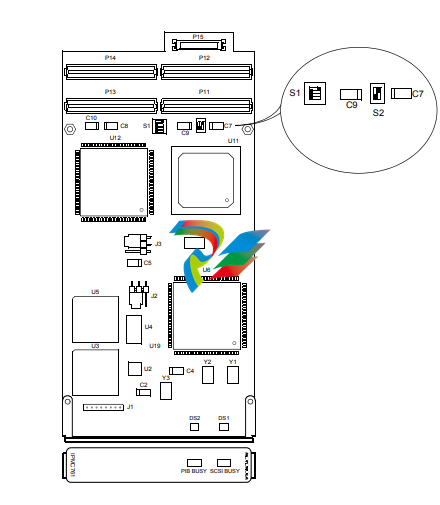
Table 1-1. IPMC761 Jumpers
Jumper Description Setting
J1 Reserved 9PLD programming
header
N/A
J2 Port 3 Transmit Clock 1-2: driven by IPMC761
2-3: received by IPMC761
J3 Port 4 Transmit Clock 1-2: driven by IPMC761
2-3: received by IPMC761
Figure 1-2. IPMC761 Functional Block Diagram
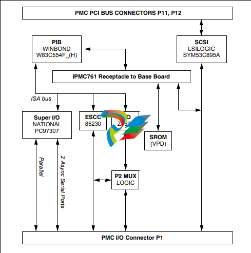
Figure 1-3. IPMC712 with Default Switch Settings
Table 1-2. IPMC712 Jumpers
Jumper Description Setting
J1 Reserved 9PLD programming
header
N/A
J2 Port 4 Receive Clock 1-2: driven by IPMC712
2-3: received by IPMC712
J3 Port 4 Transmit Clock 1-2: driven by IPMC712
2-3: received by IPMC712
J5 Clock Loopback MAX207 14/15in connects to R1out
Figure 1-4. IPMC712 Functional Block Layout
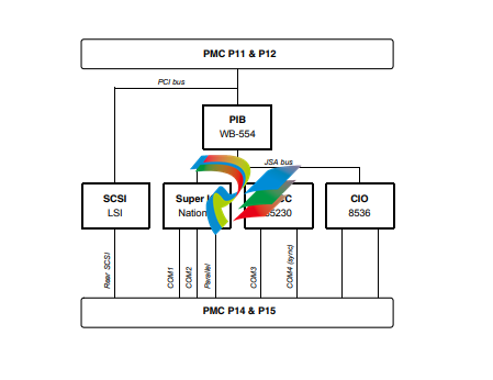
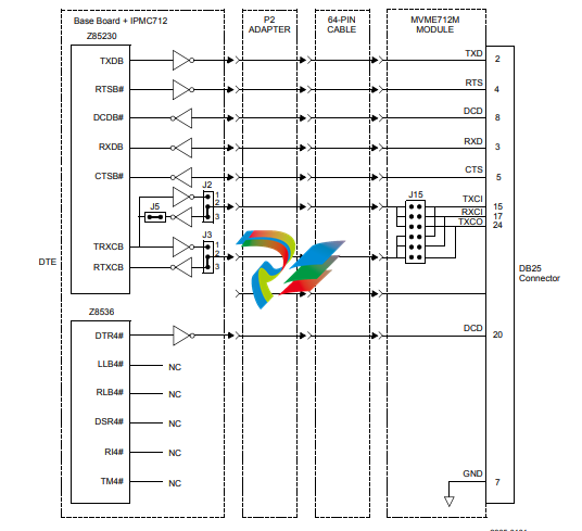
Figure 1-5. IPMC712 Serial Port 4 Clock Configuration
ISA Local Resource Bus
PCI-to-ISA Bridge (PIB)
The PIB (W83C554F) contains the ISA Bridge I/O Registers necessary for various functions.
These registers are also accessible from the PCI bus.
Super I/O
The Super I/O device (PC97307) provides the following functions on the IPMC:
■ Two synchronous serial ports (COM1 and COM2)
■ Parallel printer port
ESCC
Two DTE synchronous/asynchronous serial ports are provided by the ESCC device (Z85230).
Since the Z85230 device does not have all modem control lines, a Z8536 CIO device (described
below) is used to provide the missing lines.
A PAL device is used to perform decode for the Z85230 and the Z8536 for register accesses
and pseudo interrupt acknowledge cycles in the ISA I/O space. DMA supports for the Z85230
is provided by the PIB.
The clock input to the Z85230 PCLK pin is a 10 MHz clock. The Z85230 supplies an interrupt
vector during a pseudo interrupt acknowledge cycle. The vector is modified based upon the
interrupt source within the device.
All modem control lines from the ESCC are multiplexed/demultiplexed through connector P2 by
the P2MX function due to pin limitation of the connector.
CIO
The CIO device (Z8536) is used to provide the modem control lines not provided by the Z85230
ESCC. In addition, the device has three independent 16-bit counters/timers. The clock input to
the Z8536 PCLK pin is a 5 MHz clock.
Static ROM (SROM)
Both modules contains one +3.3V, 256 x 8 serial EEPROM device (AT24C02) onboard. This
device provides for Vital Product Data (VPD) storage of the module hardware configuration. The
serial EEPROM is located on the baseboard’s I2C bus at address $A4.
Input/Output Modes
Both modules are designed to be plugged into PMC slot 1 of the base board. As stated earlier,
these SBCs have two P2 I/O modes (IPMC and PMC) that are user configurable. The user
should configure the baseboard for the IPMC module being used.
The jumpers route the on-board Ethernet port 2 to row C of connector P2. When used, both
modules are backwards compatible with the MVME761 rear transition module and P2 adapter
card (excluding PMC I/O routing) used on the MVME2600/2700. The rear panel Ethernet is not
available when using the IPMC712.
LEDs
Both modules use two LEDs to provide PMC status.
■ The module’s green SCSI LED is lit when the SCSI device is Master
■ The module’s green PIB LED is lit when the PCI bus grant to the PIB is asserted
PCI Signaling Voltage Level
Both modules will operate with only +5V signaling levels.
RS232 Interface
On the IPMC712 module, the four serial ports are used to communicate at RS232 voltage levels
(P14). The first three ports are fixed asynchronous ports, while the remaining port can be
configured as either a synchronous or an asynchronous port.
For additional handshaking signals, the IPMC712 module has the following features:
■ Port 1 has RTS and CTS
■ Ports 2, 3, and 4 have RTS, CTS, DTR, DCD
■ Port 4 has configurable serial clock signals RTxC and TRxC
Jumpers J2, J3 and J5 determine the sources for these two signals, refer to Figure 1-5 on
page 7.
This chapter discusses the configuration and installation of IPMC modules on an MVME6100,
MVME5500, or MVME5100 SBCs.
For additional information pertaining to the MVME51005E, refer to the information contained in
the MVME51005E Single Board Computer Installation and Use manual before proceeding with
these instructions contained in this chapter.
Packaging
As a precautionary measure, IPMC modules are sealed in an anti-static package to protect
them from static discharge. Observe standard handling practices of static sensitive equipment.
Configuring the IPMC Modules
There are two user configurable switches on the IPMC712 and IPMC761 I/O modules. Switches
S1 and S2 are described in Chapter 3, Programming.
Installing IPMC Modules on Host Board
Both the IPMC712 and the IPMC761 modules are installed on PMC slot 1 of the host board. As
a general reminder, IPMC modules must be installed on the host board prior to installing it into
-
 Hirschmann RS20-1600M2T1SDAEHH03.1.02 Rail Switch
 -
 Hirschmann BRS30-24TX Industrial Rail Switch
 -
 Hirschmann RSPM20-4T14T1EV9HHS999.9.99 Managed Ethernet Switch
 -
 Hirschmann BELDEN RS40-0009CCCCSDAPHH09.0.14 / RS400009CCCCSDAPHH09014
 -
Hirschmann RS40 Rail Switch RS40-0009CCCCSDAE
-
 Hirschmann BELDEN RS30-0802T1T1SDAP / RS300802T1T1SDAP Fully Managed Layer 2 Compact Rail Switch
 -
 Hirschmann BELDEN RS20-0800M2M2SDAUHH / RS200800M2M2SDAUHH
 -
 Hirschmann EAGLE30-04022O6TT999SCCY9HSE3F Industrial Firewall Router Switch
 -
 Hirschmann RS20-1600T1T1SDAEHH09.0.14 RS20 Rail Mount Ethernet Switch
 -
 Hirschmann EAGLE0200T1T1TDDY90000HHE05.3.03 Industrial Security Router
 -
Hirschmann - BELDEN MIPP-AD-1L9P
-
 HIRSCHMANN RSPM20-4Z64Z6TV9HHS9 942 106-999 RAIL SAFETY SWITCH
 -
 HIRSCHMANN FIBEROPTIC MODULE FIP P/N: OZDFIPG3T
 -
 HIRSCHMANN RS20-1600M2M2SDAUHH Ethernet rack-mounted switch
 -
 HIRSCHMANN BELDEN RS20-0400T1T1SDAEHH04.0.01 / RS200400T1T1SDAEHH04001
 -
HIRSCHMANN MM2-4FXM3 MICE Media Module
-
HIRSCHMANN RS20-0800M2M2SDAE Industrial Ethernet Rail Switch
-
 Hirschmann RS20-2400T1T1SDAP / RS20-2400T1T1SDAPHH05.0.02
 -
 GE MLJ1005B010H00C MLJ Digital Synchromism Check
 -
 ALSTOM MICROTECH DX21-M2 Digital Excitation Controller
 -
HIRSCHMANN BRS20-1200ZZZZ-STCY99HHSES
-
 HIRSCHMANN MM3-4FXM2 MICE Media Module
 -
Hirschmann RSB20-0800T1T1SAABHH 8Port ENet Rail Switch RSB20
-
 Hirschmann MACH102-8TP Ethernet Switch
 -
 SAACKE DDZ-M marine steam pressure atomizer
 -
 SAACKE SKV-A marine rotary cup atomizer
 -
 SAACKE Seavis HMI05e
 -
 Kollmorgen MMC-SD-2.0-230 Servo Drive 100-240VAC 2KW 10A Output 3PH 100-240VAC
 -
 Kollmorgen Servo drive CR10550
 -
 Kollmorgen AKD-P01207-NACN-0054 Servo Driver
 -
 Kollmorgen S406M-CA-036 Servostar
 -
.png) Kollmorgen AKD-B02407-NAAN-0000 Digital Servo Drive
Kollmorgen AKD-B02407-NAAN-0000 Digital Servo Drive -
 Kollmorgen SERVOSTAR S406AM-CA Digital Servo Drive
 -
 KOLLMORGEN SERVOSTAR 603-AS SERVO AMPLIFIER_SERVOSTAR603AS_S60301
 -
Kollmorgen S700 Servo Controller (S70602-NANANA-NA)
-
 Kollmorgen MPK411 controller
 -
 KOLLMORGEN MMC-SD-1.3-460-D Smart Drive
 -
 KOLLMORGEN AKM21C-CKB2AA-00 / AKM21CCKB2AA00 Servomotor
 -
 BECKHOFF AX5106-0000-0200 | Digital Compact Servo Drives 1-channel
 -
 BECKHOFF C3620-0000 INDUSTRIAL COMPUTER (MOTORSHELVES)
 -
 Beckhoff EK1960-0000 TwinSAFE Compact Controller
 -
 Beckhoff C6930-0050 Control Cabinet Industrial PC
 -
 Beckhoff CP7711-0001-0030 Industrial Computer Detection
 -
 Beckhoff CX1001-0111 Embedded PC CPU Module
 -
 Beckhoff C6017-0020 | Ultra-compact Industrial PC
 -
 Beckhoff EK1322 | 2-port EtherCAT P junction with feed-in
 -
 Beckhoff CP2219-0010 Panel
 -
 BECKHOFF C6015-0020 ULTRA COMPACT INDUSTRIAL PC
 -
 BECKHOFF CX2030-0120/Standard CPU Module Embedded PC Windows PLC controller
 -
 Beckhoff CP7721-1090-0020 Panel PC
 -
 Beckhoff PC CPU Module CX5130-0175
 -
 Beckhoff C6920-0050 Control Cabinet
 -
 Beckhoff EL6631 EtherCAT 2-Port Communication Interface, Profinet RT Controller
 -
 Beckhoff CP6202-0001-0060 touch screen panel PC
 -
 Beckhoff CP3916-1002-0000 Multi-Touch Control Panel
 -
 Beckhoff EP1809-0021 | EtherCAT Box, 16-channel digital input, 24 V DC, 3 ms, M8Preferred type
 -
 Beckhoff CX8190 PLC Embedded Industrial PC Ethernet Controller
 -
 Beckhoff CX2100-0914 Power Supply for External
 -
 Beckhoff Automation CP6906-0001-0000 HMI
 -
 Beckhoff EP7342-0002 Module
 -
 Beckhoff CX1020-0112 / CX1100-0910 / CX1020-N010 / CX1100-0003 Windows CPU
 -
 Beckhoff EP7211-0034 EtherCAT Box 1 Channel Motion Interface
 -
 Beckhoff C6240-0030 Control cabinet Industrial PC
 -
 beckhoff motherboard CB1052-0004 CB1052-0004
 -
 Beckhoff AX2006-AS Servo Drive / Variable Frequency Drive
 -
BECKHOFF CP6207-0001-0020 NSMP
-
 Beckhoff C6930-1142-0060 Industrial Computer
 -
 Beckhoff FC7501-0000 interface card
 -
 Beckhoff CX5140-0175 Embedded PC PLC CPU CX5140 Industrial Controller
 -
 Beckhoff CP7802-1100-0010: High-End IP65 Control Panel with DVI/USB Extended Interface
 -
BECKHOFF CP3716-1058-0010 CONTROL PANEL
-
 Beckhoff AX8108-0000 Single-Axis Module
 -
 Beckhoff CU8851-0000 | USB extension, USB Extended 2.0 receiver box
 -
Beckhoff C6017-0030 | Ultra-compact Industrial PC
-
 Beckhoff CX1001-0120/CX10010120.cx1000-n001.cx1000-n000 System Overview
 -
 Beckhoff CPU Module CX5140-0155/4GB CPU Module
 -
 Beckhoff CP6533-0001-005: Built-in Panel PC with High-Definition Multi-Touch Control
 -
 Beckhoff EL5042 | EtherCAT Terminal, 2-channel encoder interface, BiSS® C
 -
 Beckhoff C6920-1080-0040: Premium Control Cabinet Industrial PC
 -
 Beckhoff C6920-0060 | Control cabinet Industrial PC
 -
 Beckhoff Embedded-PC CX5010-1121
 -
 Beckhoff CB3050-0010 Mainboard Motherboard
 -
 Beckhoff PLC module CX1020-0000 Basic CPU module (service phase)
 -
 Beckhoff CP7812-1056-0010 15" Multitouch Display Control Panel
 -
 Beckhoff CX5120-0115 /2GB Controller Module
 -
 Beckhoff CP7201-1000-0000 Industrial Panel PC
 -
 Beckhoff Servo Motor AM8061-0JH1-0000
 -
 BECKHOFF CP6503-0001-0050 Built-in Panel PC
 -
Beckhoff CP3919-0010 Display G190ETN01.2 19" PCT V04. Multi-touch Control Panel
-
 Beckhoff CX5110-0112-9020/000368201 Embedded PC Intel Atom Processor
 -
 Beckhoff AX8206-0000 Dual-Axis Module
 -
Beckhoff Nail Operating Terminal CP7032-1031-0010
-
Beckhoff AM8042-0EH1-0000 Servomotor 4.10 Nm (M0), F4 (87 mm)
-
 Beckhoff EK9300 Beckhoff CPU Module
 -
Beckhoff CP3224-0020 Multitouch-Panel-PC
-
 Beckhoff CP2712-0000 12.1" 24VDC Touch Screen WMD0
 -
 BECKHOFF CX5240-0195 / 0000289234 Embedded PC 40 GB CFast Card
 -
 Beckhoff CP6932-1000-0000 Control Panel
 -
 BECKHOFF CX5120-0121 PLC Module
 -
 Beckhoff EL3218 | EtherCAT Terminal, 8-channel analog input
 -
Beckhoff C6640-0050 | Control cabinet Industrial PC
-
 Beckhoff Cx5130-0120/4GB Embedded-PC
 -
 BECKHOFF CX2030-0122 PLC PROCESSOR
 -
 BECKHOFF CX5020-0122 Controller Module
 -
 Beckhoff CP3915-0000 Multitouch Panel
 -
 BECKHOFF EL3014 | EtherCAT Terminal
 -
 BECKHOFF Industrial Computer c6920-1057-0030
 -
 Beckhoff CX5130-0141/4GB CX5130-0141 Embedded PC
 -
 Beckhoff C6240-1052-0040 4-086-06-3073 Industrial Computer
 -
 Beckhoff CX5140-0135 /4GB High-Performance Embedded Industrial PC
 -
 Beckhoff C6515-1001-0000 Industrial PC
 -
 Beckhoff AX5103-0000-0200 - Digital Compact Servo Drives
 -
 Beckhoff CX2030-0130-1003/4GB Basic CPU module
 -
 Beckhoff AX8620-0000 Power Supply Module
 -
 Beckhoff CX9020-0111 module with
 -
 Beckhoff EL7332 PLC Module
 -
 BECKHOFF CP7709-0001-0020 HMI
 -
 Beckhoff CX5120-0155/2GB Embedded PC
 -
 BECKHOFF CP7037-1037-0010 OPERATOR INTERFACE TOUCHSCREEN
 -
 Beckhoff EK9000 | ModbusTCP/UDP Bus Coupler
 -
 Beckhoff Touch Panel Screen CP6020 -0000-0000
 -
 Beckhoff CX2020-0121 Module FAST Shipping
 -
 Beckhoff CX2030-0125 Basic CPU Module
 -
 Beckhoff CP3918-0000 Multi-Touch 18.5" Control Panel
 -
 Automotion LC4A00010 DC BL Motor Control, ATS, Sub Assy, SCP, 115VAC,
 -
 500T-115VAC - VAS ENGINEERING - DORIC 500 SERIES DIGITAL TEMP INDICATOR
 -
 Honeywell X-DCS2000/EN Digital Integrated System Manager 50/60Hz 100-240V #4
 -
 Kollmorgen S60600 Servostar600 606-Fan 4 kVA, 6 A, 3 X 230 - 480 V